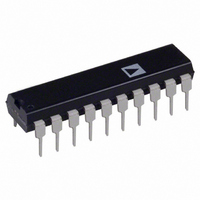
AD7248JNZ Analog Devices Inc, AD7248JNZ Datasheet - Page 9

AD7248JNZ
Manufacturer Part Number
AD7248JNZ
Description
IC DAC 12BIT W/REF 20-DIP
Manufacturer
Analog Devices Inc
Series
DACPORT®r
Datasheet
1.AD7245AARZ.pdf
(16 pages)
Specifications of AD7248JNZ
Data Interface
Parallel
Settling Time
7µs
Number Of Bits
12
Number Of Converters
1
Voltage Supply Source
Dual ±
Power Dissipation (max)
210mW
Operating Temperature
-40°C ~ 85°C
Mounting Type
Through Hole
Package / Case
20-DIP (0.300", 7.62mm)
Resolution (bits)
12bit
Input Channel Type
Parallel
Supply Current
5mA
Digital Ic Case Style
DIP
No. Of Pins
20
Operating Temperature Range
0°C To +70°C
Lead Free Status / RoHS Status
Lead free / RoHS Compliant
Available stocks
Company
Part Number
Manufacturer
Quantity
Price
Company:
Part Number:
AD7248JNZ
Manufacturer:
SYNCMOS
Quantity:
6 217
The data held in the DAC latch determines the analog output of
the converter. Data is latched into the DAC latch on the rising
edge of LDAC. This LDAC signal is an asynchronous signal
and is independent of WR. This is useful in many applications.
However, in systems where the asynchronous LDAC can occur
during a write cycle (or vice versa) care must be taken to ensure
that incorrect data is not latched through to the output. For
example, if LDAC goes LOW while WR is “LOW,” then the
LDAC signal must stay LOW for t
high to ensure correct data is latched through to the output.
CLR
H
H
H
H
H
H
H
L
g
g
H = High State, L = Low State, X = Don’t Care
The contents of the DAC latch are reset to all 0s by a low level
on the CLR line. With both latches transparent, the CLR line
functions like a zero override with the output brought to 0 V in
the unipolar mode and –5 V in the bipolar mode for the dura-
tion of the CLR pulse. If both latches are latched, a “LOW”
pulse on the CLR input latches all 0s into the DAC latch and the
output remains at 0 V (or –5 V) after the CLR line has returned
“HIGH.” The CLR line can be used to ensure power-up to 0 V
on the AD7245A output in unipolar operation and is also use-
ful, when used as a zero override, in system calibration cycles.
Figure 4 shows the input control logic for the AD7245A and the
write cycle timing for the part is shown in Figure 5.
LDAC WR
L
H
H
H
H
L
g
X
H
L
LDAC
CLR
WR
CS
Table I. AD7245A Truth Table
L
H
X
L
g
H
H
X
H
L
CS
L
X
H
L
L
H
H
X
H
L
Function
Both Latches are Transparent
Both Latches are Latched
Both Latches are Latched
Input Latches Transparent
Input Latches Latched
DAC Latches Transparent
DAC Latches Latched
DAC Latches Loaded with all 0s
DAC Latches Latched with All
0s and Output Remains at
0 V or –5 V
Both Latches are Transparent
and Output Follows Input Data
7
or longer after WR goes
INPUT LATCH
DAC LATCH
INPUT DATA
INTERFACE LOGIC INFORMATION—AD7248A
The input loading structure on the AD7248A is configured for
interfacing to microprocessors with an 8-bit wide data bus. The
part contains two 12-bit latches—an input latch and a DAC
latch. Only the data held in the DAC latch determines the ana-
log output from the converter. The truth table for AD7248A
operation is shown in Table II, while the input control logic
diagram is shown in Figure 6.
CSMSB, CSLSB and WR control the loading of data from the
external data bus to the input latch. The eight data inputs on
the AD7248A accept right justified data. This data is loaded to
the input latch in two separate write operations. CSLSB and
WR control the loading of the lower 8-bits into the 12-bit wide
latch. The loading of the upper 4-bit nibble is controlled by
CSMSB and WR. All control inputs are level triggered, and
input data for either the lower byte or upper 4-bit nibble is
latched into the input latches on the rising edge of WR (or
either CSMSB or CSLSB). The order in which the data is
loaded to the input latch (i.e., lower byte or upper 4-bit nibble
first) is not important.
LDAC
DATA
WR
CS
t
3
NOTES
1. SEE TIMING SPECIFICATIONS.
2. ALL INPUT RISE AND FALL TIMES MEASURES FROM 10% TO
3. TIMING MEASUREMENT REFERENCE LEVEL IS
4. IF LDAC IS ACTIVATED WHILE WR IS LOW, LDAC MUST STAY
CSMSB
CSLSB
90% OF 5V,
LOW FOR
LDAC
WR
V
INH
+ V
2
t
t
t
7
t
1
2
t
r
OR LONGER AFTER WR GOES HIGH.
5
VALID
INL
=
DATA
t
f
= 5ns.
t
6
t
4
AD7245A/AD7248A
OF INPUT
UPPER
LATCH
4 BITS
4
HIGH IMPEDANCE
DAC LATCH
DB7 – DB0
BUS
12
8
t
OF INPUT
7
LOWER
8 BITS
LATCH
8
5V
0V
5V
5V
0V
5V
0V
0V


