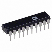
AD7248JNZ Analog Devices Inc, AD7248JNZ Datasheet - Page 11

AD7248JNZ
Manufacturer Part Number
AD7248JNZ
Description
IC DAC 12BIT W/REF 20-DIP
Manufacturer
Analog Devices Inc
Series
DACPORT®r
Datasheet
1.AD7245AARZ.pdf
(16 pages)
Specifications of AD7248JNZ
Data Interface
Parallel
Settling Time
7µs
Number Of Bits
12
Number Of Converters
1
Voltage Supply Source
Dual ±
Power Dissipation (max)
210mW
Operating Temperature
-40°C ~ 85°C
Mounting Type
Through Hole
Package / Case
20-DIP (0.300", 7.62mm)
Resolution (bits)
12bit
Input Channel Type
Parallel
Supply Current
5mA
Digital Ic Case Style
DIP
No. Of Pins
20
Operating Temperature Range
0°C To +70°C
Lead Free Status / RoHS Status
Lead free / RoHS Compliant
Available stocks
Company
Part Number
Manufacturer
Quantity
Price
Company:
Part Number:
AD7248JNZ
Manufacturer:
SYNCMOS
Quantity:
6 217
UNIPOLAR (0 V TO 5 V) CONFIGURATION
The 0 V to 5 V output voltage range is achieved by tying R
R
AD7248A can be operated single supply (V
ply. The table for output voltage versus digital code is as in Table
III, with 2 × V
BIPOLAR CONFIGURATION
The bipolar configuration for the AD7245A/AD7248A, which
gives an output voltage range from –5 V to +5 V, is achieved by
connecting the R
and V
dual supplies to achieve this output voltage range. The code
table for bipolar operation is shown in Table IV.
DAC Latch Contents
MSB
1 1 1 1
1 0 0 0
1 0 0 0
0 1 1 1
0 0 0 0
0 0 0 0
NOTE: 1 LSB = 2 × V
AGND BIAS
The AD7245A/AD7248A AGND pin can be biased above sys-
tem GND (AD7245A/AD7248A DGND) to provide an offset
“zero” analog output voltage level. With unity gain on the
amplifier (R
expressed as:
where D is a fractional representation of the digital word in the
DAC latch and V
AD7248A AGND pin.
Because the current flowing out of the AGND pin varies with
digital code, the AGND pin should be driven from a low imped-
ance source. A circuit configuration is outlined for AGND bias
in Figure 9 using the AD589, a +1.23 V bandgap reference.
If a gain of 2 is used on the buffer amplifier the output voltage,
V
FB
OUT
and V
is expressed as
OUT
1 LSB = V
. The AD7245A/AD7248A must be operated from
OUT
1 1 1 1
0 0 0 0
0 0 0 0
1 1 1 1
0 0 0 0
0 0 0 0
OFS
REF
together. For this output range the AD7245A/
= V
Table IV. Bipolar Code Table
OFS
V
BIAS
replaced by V
V
OUT
REF
OUT
OUT
input to REF OUT and connecting R
is the voltage applied to the AD7245A/
(2
LSB
1 1 1 1
0 0 0 1
0 0 0 0
1 1 1 1
0 0 0 1
0 0 0 0
= 2(V
REF
= R
–12
= V
) = V
(2
FB
BIAS
BIAS
–11
) the output voltage, V
) = V
REF
REF
+ D
Analog Output, V
+V
+V
–V
–V
–V
+ D
. Note that for this range
REF
REF
REF
REF
REF
REF
0 V
×
×
×
V
×
×
4096
V
SS
REF
1
REF
2048
= 0 V) or dual sup-
2048
2047
2048
2048
2048
2047
2048
2048
1
1
)
1
.
= –V
OUT
OUT
REF
OFS
is
FB
,
In this case care must be taken to ensure that the maximum
output voltage is not greater than V
overhead must be greater than 3 V to ensure correct operation
of the part. Note that V
must be referenced to DGND (system GND). The entire circuit
can be operated in single supply with the V
AD7245A/AD7248A connected to system GND.
V
PROGRAMMABLE CURRENT SINK
Figure 10 shows how the AD7245A/AD7248A can be config-
ured with a power MOSFET transistor, the VN0300M, to
provide a programmable current sink from V
The VN0300M is placed in the feedback of the AD7245A/
AD7248A amplifier. The entire circuit can be operated in single
supply by tying the V
The sink current, I
0.1 F
Using the VN0300M, the voltage drop across the load can typi-
cally be as large as V
5 V. Therefore, for a current of 50 mA flowing in the R1 (with
all 1s in the DAC register) the maximum load is 200 Ω with
V
up to 500 mA and still function correctly in the circuit, but in
practice the circuit must be used with larger values of V
otherwise it requires a very small load.
BIAS
SOURCE
27k
DIGITAL CIRCUITRY
OMITTED FOR CLARITY.
+
–
DIGITAL CIRCUITRY
OMITTED FOR CLARITY.
15V
0.1 F
AD589
AGND
= 15 V. The VN0300M can actually handle currents
+
REF
REF OUT
10 F
10
+
V
SINK
REF
REF
REF OUT
10 F
SS
SOURCE
10
, can be expressed as:
I
DD
of the AD7245A/AD7248A to AGND.
SINK
DGND
V
REF
DAC
and V
R
=
OFS
–6 V) with V
2R
AD7245A/AD7248A
AD7245A/AD7248A
DGND
D ×V
AGND
SS
DAC
R1
for the AD7245A/AD7248A
R
OFS
2R
AD7245A/AD7248A
REF
DD
V
DD
2R
–3 V. The V
OUT
SS
V
SS
V
pin of the
DD
DD
of the DAC at
2R
R
V
OUT
or V
FB
V
SS
DD
V
SOURCE
SOURCE
SOURCE
–V
R
V
FB
OUT
LOAD
VN0300M
OUT
R1
SYSTEM
I
SINK
GND
.


