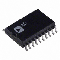
AD7528JRZ Analog Devices Inc, AD7528JRZ Datasheet - Page 4

AD7528JRZ
Manufacturer Part Number
AD7528JRZ
Description
IC DAC 8BIT DUAL MULT 20-SOIC
Manufacturer
Analog Devices Inc
Datasheet
1.AD7528KNZ.pdf
(8 pages)
Specifications of AD7528JRZ
Settling Time
400ns
Number Of Bits
8
Number Of Converters
2
Voltage Supply Source
Single Supply
Power Dissipation (max)
450mW
Operating Temperature
-40°C ~ 85°C
Mounting Type
Surface Mount
Package / Case
20-SOIC (7.5mm Width)
Resolution (bits)
8bit
Sampling Rate
5.6MSPS
Input Channel Type
Parallel
Supply Current
2mA
Digital Ic Case Style
SOIC
No. Of Pins
20
Data Interface
Parallel
Lead Free Status / RoHS Status
Lead free / RoHS Compliant
Lead Free Status / RoHS Status
Lead free / RoHS Compliant, Lead free / RoHS Compliant
Available stocks
Company
Part Number
Manufacturer
Quantity
Price
Company:
Part Number:
AD7528JRZ
Manufacturer:
Analog Devices Inc
Quantity:
135
Part Number:
AD7528JRZ
Manufacturer:
ADI/亚德诺
Quantity:
20 000
Part Number:
AD7528JRZ-REEL
Manufacturer:
ADI/亚德诺
Quantity:
20 000
AD7528
INTERFACE LOGIC INFORMATION
DAC Selection:
Both DAC latches share a common 8-bit input port. The con-
trol input DAC A/DAC B selects which DAC can accept data
from the input port.
Mode Selection:
Inputs CS and WR control the operating mode of the selected
DAC. See Mode Selection Table below.
Write Mode:
When CS and WR are both low the selected DAC is in the write
mode. The input data latches of the selected DAC are transpar-
ent and its analog output responds to activity on DB0–DB7.
Hold Mode:
The selected DAC latch retains the data which was present on
DB0–DB7 just prior to CS or WR assuming a high state. Both
analog outputs remain at the values corresponding to the data in
their respective latches.
DAC A/DAC B
L
H
X
X
L = Low State; H = High State; X = Don’t Care.
WRITE CYCLE TIMING DIAGRAM
CIRCUIT INFORMATION—D/A SECTION
The AD7528 contains two identical 8-bit multiplying D/A con-
verters, DAC A and DAC B. Each DAC consists of a highly
stable thin film R-2R ladder and eight N-channel current steer-
ing switches. A simplified D/A circuit for DAC A is shown in
CHIP SELECT
DAC A/DAC B
(DB0 – DB7)
DATA IN
Figure 1. Simplified Functional Circuit for DAC A
WRITE
V
REF
A
NOTES:
1. ALL INPUT SIGNAL RISE AND FALL TIMES MEASURED
2. TIMING MEASUREMENT REFERENCE LEVEL IS
FROM 10% TO 90% OF V
V
V
DD
DD
DAC A DATA LATCHES
2R
S1
= +5V,
= +15V,
R
CS
L
L
H
X
AND DRIVERS
Mode Selection Table
t
S2
2R
r =
t
r =
R
t
f = 20ns;
t
f = 40ns;
V
V
S3
2R
IH
IL
t
t
WR
L
L
X
H
CS
AS
DATA IN STABLE
R
t
DD
WR
t
DS
.
S8
2R
2R
DAC A
WRITE
HOLD
HOLD
HOLD
t
t
R
CH
AH
R
OUT A
AGND
t
DH
FB
V
A
IH
+ V
2
DAC B
HOLD
WRITE
HOLD
HOLD
IL
0
0
0
0
V
V
V
V
DD
DD
DD
DD
–4–
Figure 1. An inverted R-2R ladder structure is used, that is, bi-
nary weighted currents are switched between the DAC output
and AGND thus maintaining fixed currents in each ladder leg
independent of switch state.
EQUIVALENT CIRCUIT ANALYSIS
Figure 2 shows an approximate equivalent circuit for one of the
AD7528’s D/A converters, in this case DAC A. A similar
equivalent circuit can be drawn for DAC B. Note that AGND
(Pin 1) is common for both DAC A and DAC B.
The current source I
tion leakages and, as with most semiconductor devices, approxi-
mately doubles every 10 C. The resistor R
2 is the equivalent output resistance of the device which varies
with input code (excluding all 0s code) from 0.8 R to 2 R. R is
typically 11 k . C
switches and varies from about 50 pF to 120 pF depending
upon the digital input. g(V
voltage generator due to the reference input voltage V
the transfer function of the R-2R ladder.
CIRCUIT INFORMATION–DIGITAL SECTION
The input buffers are simple CMOS inverters designed such
that when the AD7528 is operated with V
converts TTL input levels (2.4 V and 0.8 V) into CMOS logic
levels. When V
input buffers operate in their linear region and pass a quiescent
current, see Figure 3. To minimize power supply currents it is
recommended that the digital input voltages be as close to the
supply rails (V
The AD7528 may be operated with any supply voltage in the
range 5
levels are CMOS compatible only, i.e., 1.5 V and 13.5 V.
Figure 3. Typical Plots of Supply Current, I
Input Voltage V
Figure 2. Equivalent Analog Output Circuit of DAC A
800
700
600
500
400
300
200
100
0
V
g(V
V
DD
DD
1
REF
DD
= +5V
IN
A, N)
2
15 volts. With V
is in the region of 2.0 volts to 3.5 volts the
V
and DGND) as is practically possible.
OUT
DD
IN
3
, for V
LEAKAGE
= +15V
is the capacitance due to the N-channel
4
R
O
5
REF
DD
is composed of surface and junc-
6
V
= +5 V and +15 V
IN
A, N) is the Thevenin equivalent
– Volts
I
7
LKG
DD
8
= +15 V the input logic
T
ALL DIGITAL INPUTS
TIED TOGETHER
A
9
R
C
= +25 C
OUT
DD
10 11
O
as shown in Figure
= 5 V, the buffer
R
OUT A
AGND
FB
12
DD
A
vs. Logic
13
REF
14
9
8
7
6
5
4
3
2
1
REV. B
A and


