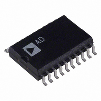
AD7528JRZ Analog Devices Inc, AD7528JRZ Datasheet - Page 2

AD7528JRZ
Manufacturer Part Number
AD7528JRZ
Description
IC DAC 8BIT DUAL MULT 20-SOIC
Manufacturer
Analog Devices Inc
Datasheet
1.AD7528KNZ.pdf
(8 pages)
Specifications of AD7528JRZ
Settling Time
400ns
Number Of Bits
8
Number Of Converters
2
Voltage Supply Source
Single Supply
Power Dissipation (max)
450mW
Operating Temperature
-40°C ~ 85°C
Mounting Type
Surface Mount
Package / Case
20-SOIC (7.5mm Width)
Resolution (bits)
8bit
Sampling Rate
5.6MSPS
Input Channel Type
Parallel
Supply Current
2mA
Digital Ic Case Style
SOIC
No. Of Pins
20
Data Interface
Parallel
Lead Free Status / RoHS Status
Lead free / RoHS Compliant
Lead Free Status / RoHS Status
Lead free / RoHS Compliant, Lead free / RoHS Compliant
Available stocks
Company
Part Number
Manufacturer
Quantity
Price
Company:
Part Number:
AD7528JRZ
Manufacturer:
Analog Devices Inc
Quantity:
135
Part Number:
AD7528JRZ
Manufacturer:
ADI/亚德诺
Quantity:
20 000
Part Number:
AD7528JRZ-REEL
Manufacturer:
ADI/亚德诺
Quantity:
20 000
Parameter
STATIC PERFORMANCE
DIGITAL INPUTS
SWITCHING CHARACTERISTICS
POWER SUPPLY
AC PERFORMANCE CHARACTERISTICS
Parameter
DC SUPPLY REJECTION ( GAIN/ V
CURRENT SETTLING TIME
PROPAGATION DELAY (From Digital In-
DIGITAL-TO-ANALOG GLITCH IMPULSE All
OUTPUT CAPACITANCE
AC FEEDTHROUGH
AD7528–SPECIFICATIONS
Resolution
Relative Accuracy
Differential Nonlinearity
Gain Error
Gain Temperature Coefficient
Output Leakage Current
Input Resistance (V
V
Input High Voltage
Input Low Voltage
Input Current
Input Capacitance
Chip Select to Write Set Up Time
Chip Select to Write Hold Time
DAC Select to Write Set Up Time
DAC Select to Write Hold Time
Data Valid to Write Set Up Time
Data Valid to Write Hold Time
Write Pulsewidth
I
put to 90% of Final Analog Output Current) All
C
C
C
C
V
V
DD
REF
REF
REF
OUT
OUT
OUT
OUT
OUT A (Pin 2)
OUT B (Pin 20)
Match
V
V
I
DB0–DB7
WR, CS, DAC A/DAC B
t
t
t
t
t
t
t
CS
CH
AS
AH
DS
DH
WR
IN
Gain/ Temperature
IH
IL
A/V
A to OUT A
A
B
A
B
B to OUT B
REF
B Input Resistance
4
REF
6
A, V
2
REF
2
3
B)
3
DD
)
Version
All
J, A, S
K, B, T
L, C, U
All
J, A, S
K, B, T
L, C, U
All
All
All
All
All
All
All
All
All
All
All
All
All
All
All
All
All
All
All
Version
All
All
All
All
1
T
8
8
15
2.4
0.8
10
15
90
0
90
0
80
0
90
2
100
1
1/2
1/2
1
4
2
1
0.007
50
50
1
1
A
1
= +25 C T
T
0.02
350
220
160
50
50
120
120
–70
–70
V
A
DD
= +25 C T
= +5 V
V
DD
8
8
0.8
100
100
0
100
2
500
15
2.4
10
15
0
0
90
(V
1
1/2
1/2
1
6
4
3
0.007
400
400
1
10
MIN
= +5 V
REF
, T
0.04
400
270
50
50
120
120
–65
–65
5
A = V
MIN
MAX
(Measured Using Recommended P.C. Board Layout (Figure 7) and AD644 as
Output Amplifiers)
, T
MAX
REF
T
8
8
15
13.5
1.5
10
15
60
10
60
10
30
0
60
2
100
–2–
1
1/2
1/2
1
4
2
1
0.0035
50
50
1
1
A
B = +10 V; OUT A = OUT B = O V unless otherwise noted)
= +25 C T
T
0.01
180
80
440
50
50
120
120
–70
–70
A
V
= +25 C T
DD
V
DD
= +15 V
8
8
15
13.5
1.5
10
15
80
15
80
15
40
0
80
2
500
= +15 V
1
1/2
1/2
1
5
3
1
0.0035
200
200
1
10
MIN
0.02
200
100
50
50
120
120
–65
–65
MIN
, T
MAX
, T
MAX
Units
Bits
LSB max
LSB max
LSB max
LSB max
LSB max
LSB max
LSB max
%/ C max
nA max
nA max
k min
k max
% max
V min
V max
pF max
pF max
ns min
ns min
ns min
ns min
ns min
ns min
ns min
mA max
Units
% per % max
ns max
ns max
nV sec typ
pF max
pF max
pF max
pF max
dB max
dB max
A max
A max
Test Conditions/Comments
This is an Endpoint Linearity Specification
All Grades Guaranteed Monotonic Over
Full Operating Temperature Range
Measured Using Internal R
Both DAC Latches Loaded with 11111111
Gain Error is Adjustable Using Circuits
of Figures 4 and 5
DAC Latches Loaded with 00000000
Input Resistance TC = –300 ppm/ C, Typical
Input Resistance is 11 k
V
See Timing Diagram
See Figure 3
All Digital Inputs V
All Digital Inputs 0 V or V
IN
Test Conditions/Comments
To 1/2 LSB. OUT A/OUT B Load = 100
WR = CS = 0 V. DB0–DB7 = 0 V to V
V
V
OUT A, OUT B Load = 100
WR = CS = 0 V DB0–DB7 = 0 V to V
V
For Code Transition 00000000 to 11111111
DAC Latches Loaded with 00000000
DAC Latches Loaded with 11111111
V
@ 100 kHz
V
DD
REF
DD
REF
= 0 or V
DD
to 0 V
to 0 V
A = V
A, V
= 5%
REF
DD
REF
B = 20 V p-p Sine Wave
B = +10 V
IL
or V
IH
DD
FB
A and R
C
EXT
FB
REV. B
= 13 pF
DD
B
DD
or
or
.


