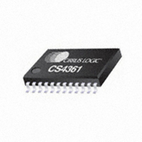
CS4361-CZZ Cirrus Logic Inc, CS4361-CZZ Datasheet - Page 16

CS4361-CZZ
Manufacturer Part Number
CS4361-CZZ
Description
IC DAC STER 6CH 103DB 20TSSOP
Manufacturer
Cirrus Logic Inc
Datasheet
1.CS4361-CZZ.pdf
(24 pages)
Specifications of CS4361-CZZ
Package / Case
20-TSSOP
Number Of Bits
24
Data Interface
Serial
Number Of Converters
6
Voltage Supply Source
Single Supply
Power Dissipation (max)
455mW
Operating Temperature
-40°C ~ 85°C
Mounting Type
Surface Mount
Conversion Rate
192 KSPS
Resolution
24 bit
Interface Type
Serial
Operating Supply Voltage
3.3 V or 5 V
Operating Temperature Range
+ 85 C
Maximum Power Dissipation
455 mW
Mounting Style
SMD/SMT
Number Of Dac Outputs
6
Lead Free Status / RoHS Status
Lead free / RoHS Compliant
For Use With
598-1153 - BOARD EVAL FOR CS4361428-1454 - SOCKET ADAPTER FOR CY2077FZ
Settling Time
-
Lead Free Status / Rohs Status
Lead free / RoHS Compliant
Other names
598-1057-5
Available stocks
Company
Part Number
Manufacturer
Quantity
Price
Part Number:
CS4361-CZZ
Manufacturer:
CIRRUS
Quantity:
20 000
Company:
Part Number:
CS4361-CZZR
Manufacturer:
HITACHI
Quantity:
923
Part Number:
CS4361-CZZR
Manufacturer:
CIRRUS
Quantity:
20 000
16
4.6
4.6.1
4.6.2
4.7
4.8
Output Transient Control
The CS4361 uses Popguard technology to minimize the effects of output transients during power-up and
power-down. When implemented with external DC-blocking capacitors connected in series with the audio
outputs, this feature eliminates the audio transients commonly produced by single-ended, single-supply
converters. To make the best use of this feature, it is necessary to understand its operation.
Grounding and Power Supply Decoupling
As with any high-resolution converter, the CS4361 requires careful attention to power supply and grounding
arrangements to optimize performance.
connected to a clean +5 V supply. For best performance, decoupling and filter capacitors should be located
as close to the device package as possible, with the smallest capacitors placed closest.
Analog Output and Filtering
The analog filter present in the CS4361 is a switched-capacitor filter followed by a continuous-time, low-
pass filter. Its response, combined with that of the digital interpolator, is given in
ommended external analog circuitry is shown in the
The analog outputs are named AOUT1-6. The SDIN1 feeds AOUT1 as the ‘Left’ marked data and AOUT2
as the ‘Right’ marked data. The SDIN2 feeds AOUT3 as the ‘Left’ marked data and AOUT4 as the ‘Right’
marked data. The SDIN3 feeds AOUT5 as the ‘Left’ marked data and AOUT6 as the ‘Right’ marked data.
Power-Up
When the device is initially powered up, the audio outputs, AOUT1-6, are clamped to VQ, which is initially
low. After RST is released and MCLK is applied, the outputs begin to ramp with VQ towards the nominal
quiescent voltage. This ramp takes approximately 200 ms to complete. The gradual voltage ramping al-
lows time for the external DC-blocking capacitors to charge to VQ, effectively blocking the quiescent DC
voltage. Audio output begins approximately 2000 sample periods after valid LRCK and SDIN are supplied
(and SCLK, if used).
Power-Down
To prevent audio transients at power-down, the DC-blocking capacitors must fully discharge before turn-
ing off the power. In order to do this, either stop MCLK or hold RST low for a period of about 250 ms before
removing power. During this time, voltage on VQ and the audio outputs discharge gradually to GND. If
power is removed before this 250 ms time period has passed, a transient will occur when the VA supply
drops below that of VQ. There is no minimum time for a power cycle; power may be reapplied at any time.
When changing clock ratio or sample rate, it is recommended that zero data (or near zero data) be present
on SDIN for at least 10 LRCK samples before the change is made. During the clocking change, the DAC
outputs will always be in a zero data state. If non-zero audio is present at the time of switching, a slight
click or pop may be heard as the DAC output automatically goes to its zero data state.
Confidential Draft
Figure 6
2/12/08
shows the recommended power arrangement, with VA
“Typical Connection Diagram” on page
Figures 14
11.
- 21. The rec-
CS4361


