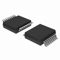
UDA1330ATS/N2,112 NXP Semiconductors, UDA1330ATS/N2,112 Datasheet - Page 5

UDA1330ATS/N2,112
Manufacturer Part Number
UDA1330ATS/N2,112
Description
IC AUDIO DAC STEREO 16-SSOP
Manufacturer
NXP Semiconductors
Datasheet
1.UDA1330ATSN2118.pdf
(23 pages)
Specifications of UDA1330ATS/N2,112
Number Of Bits
20
Data Interface
Serial
Number Of Converters
2
Voltage Supply Source
Analog and Digital
Power Dissipation (max)
75mW
Operating Temperature
-40°C ~ 85°C
Mounting Type
Surface Mount
Package / Case
16-SSOP
Lead Free Status / RoHS Status
Lead free / RoHS Compliant
Settling Time
-
Other names
568-3442-5
935262880112
UDA1330ATSDK
935262880112
UDA1330ATSDK
NXP Semiconductors
FUNCTIONAL DESCRIPTION
System clock
The UDA1330ATS operates in slave mode only.
Therefore, in all applications the system devices must
provide the system clock. The system frequency (f
selectable and depends on the application mode. The
options are: 256f
256f
must be locked in frequency to the digital interface input
signals.
The UDA1330ATS supports sampling frequencies from
8 to 55 kHz.
Application modes
The application mode can be set with the three-level
pin APPSEL (see Table 1):
• L3 mode
• Static pin mode with f
• Static pin mode with f
Table 1 Selecting application mode and system clock
The function of an application input pin (active HIGH)
depends on the application mode (see Table 2).
Table 2 Functions of application input pins
For example, in the static pin mode the output signal can
be soft muted by setting pin APPL0 to HIGH.
De-emphasis can be switched on for 44.1 kHz by setting
pin APPL1 to HIGH; setting pin APPL1 to LOW will disable
de-emphasis.
2001 Feb 02
VOLTAGE ON
PIN APPSEL
Low-cost stereo filter DAC
s
0.5V
APPL0
APPL1
APPL2
APPL3
or 384f
V
V
PIN
DDD
SSD
DDD
frequency via pin APPSEL
s
for the static pin mode. The system clock
s
, 384f
static pin mode
L3CLOCK
L3 MODE
L3MODE
L3 mode
L3DATA
s
MODE
sys
sys
TEST
and 512f
= 384f
= 256f
FUNCTION
s
s
s
.
for the L3 mode and
256f
STATIC PIN MODE
s
, 384f
DEEM
MUTE
384f
256f
SF0
SF1
f
sys
s
s
s
or 512f
sys
) is
s
5
In the L3 mode, pin APPL0 must be set to LOW. It should
be noted that when the L3 mode is used, an initialization
must be performed when the IC is powered-up.
Multiple format input interface
D
The digital interface of the UDA1330ATS supports multiple
format inputs (see Fig.3).
Left and right data-channel words are time multiplexed.
The WS signal must have a 50% duty factor for all
LSB-justified formats.
The BCK clock can be up to 64f
BCK frequency is 64 times the Word Select (WS)
frequency or less: f
Important: the WS edge MUST fall on the negative edge
of the BCK at all times for proper operation of the digital
interface.
The UDA1330ATS also accepts double speed data for
double speed data monitoring purposes
L3
This mode supports the following input formats:
• I
• MSB-justified format with data word length up to 20 bits
• LSB-justified format with data word length of
S
This mode supports the following input formats:
• I
• LSB-justified format with data word length of
These four formats are selectable via the static pin codes
SF0 and SF1 (see Table 3).
Table 3 Input format selection using SF0 and SF1
I
LSB-justified 16 bits
LSB-justified 18 bits
LSB-justified 20 bits
TATIC PIN MODE
2
ATA FORMATS
16, 18 or 20 bits.
16, 18 or 20 bits.
S-bus
2
2
MODE
S-bus format with data word length of up to 20 bits
S-bus format with data word length of up to 20 bits
FORMAT
BCK
≤ 64 × f
WS
s
, or in other words the
.
UDA1330ATS
SF0
0
0
1
1
Product specification
SF1
0
1
0
1


