UDA1334ATS/N2,112 NXP Semiconductors, UDA1334ATS/N2,112 Datasheet - Page 12
UDA1334ATS/N2,112
Manufacturer Part Number
UDA1334ATS/N2,112
Description
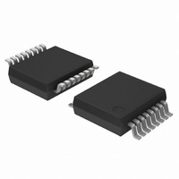
IC AUDIO DAC LP 16-SSOP
Manufacturer
NXP Semiconductors
Datasheet
1.UDA1334ATSN2112.pdf
(22 pages)
Specifications of UDA1334ATS/N2,112
Number Of Converters
2
Package / Case
16-SSOP
Number Of Bits
24
Data Interface
Serial
Voltage Supply Source
Analog and Digital
Operating Temperature
-40°C ~ 85°C
Mounting Type
Surface Mount
Interface Type
Serial
Supply Voltage (max)
3.6 V
Supply Voltage (min)
2.4 V
Maximum Operating Temperature
+ 85 C
Mounting Style
SMD/SMT
Minimum Operating Temperature
- 40 C
Lead Free Status / RoHS Status
Lead free / RoHS Compliant
Power Dissipation (max)
-
Settling Time
-
Lead Free Status / Rohs Status
Lead free / RoHS Compliant
Other names
568-3443-5
935266839112
UDA1334ATSDH
935266839112
UDA1334ATSDH


NXP Semiconductors
Notes
1. All supply connections must be made to the same external power supply unit.
2. When the DAC drives a capacitive load above 50 pF, a series resistance of 100 Ω must be used to prevent
14 AC CHARACTERISTICS
14.1
V
unless otherwise specified.
2000 Jul 31
Digital input pins: TTL compatible
V
V
⎪I
C
3-level input: pin PLL0
V
V
V
Digital output pins
V
V
DAC
V
R
I
R
C
DAC
V
ΔV
(THD + N)/S
o(max)
DDD
IH
IL
IH
IM
IL
OH
OL
ref(DAC)
o(rms)
Low power audio DAC with PLL
i
o(ref)
L
L
LI
SYMBOL
SYMBOL
o
oscillations in the output operational amplifier.
⎪
= V
Analog
DDA
= 3.0 V; f
HIGH-level input voltage
LOW-level input voltage
input leakage current
input capacitance
HIGH-level input voltage
MID-level input voltage
LOW-level input voltage
HIGH-level output voltage
LOW-level output voltage
reference voltage
output resistance on
pin V
maximum output current
load resistance
load capacitance
output voltage (RMS value)
unbalance between channels
total harmonic
distortion-plus-noise to signal
ratio
i
ref(DAC)
= 1 kHz; T
PARAMETER
PARAMETER
amb
= 25 °C; R
L
I
I
with respect to V
(THD + N)/S < 0.1%;
R
note 2
at 0 dB (FS) digital input; note 1
f
f
f
f
OH
OL
s
s
s
s
= 5 kΩ; all voltages with respect to ground (pins V
L
= 44.1 kHz; at 0 dB
= 44.1 kHz; at −60 dB; A-weighted
= 96 kHz; at 0 dB
= 96 kHz; at −60 dB; A-weighted
= 5 kΩ
= 2 mA
= −2 mA
CONDITIONS
12
CONDITIONS
SSA
2.0
−0.5
−
−
0.9V
0.4V
−0.5
0.85V
−
0.45V
−
−
3
−
MIN.
DDD
DDD
DDD
DD
−
−
−
−
−
−
−
−
−
0.5V
25
1.6
−
−
TYP.
DD
5.0
+0.8
1
10
V
0.6V
+0.5
−
0.4
0.55V
−
−
−
50
UDA1334ATS
DDD
900
0.1
−90
−40
−85
−38
Product specification
MAX.
DDD
TYP.
SSA
+ 0.5
DD
and V
V
V
μA
pF
V
V
V
V
V
V
kΩ
mA
kΩ
pF
mV
dB
dB
dB
dB
dB
SSD
UNIT
UNIT
);
Related parts for UDA1334ATS/N2,112
Image
Part Number
Description
Manufacturer
Datasheet
Request
R

Part Number:
Description:
Low Power Audio Dac With Pll
Manufacturer:
NXP Semiconductors
Datasheet:

Part Number:
Description:
IC LOW POWER AUDIO DAC 16SSOP
Manufacturer:
NXP Semiconductors
Datasheet:
Part Number:
Description:
NXP Semiconductors designed the LPC2420/2460 microcontroller around a 16-bit/32-bitARM7TDMI-S CPU core with real-time debug interfaces that include both JTAG andembedded trace
Manufacturer:
NXP Semiconductors
Datasheet:

Part Number:
Description:
NXP Semiconductors designed the LPC2458 microcontroller around a 16-bit/32-bitARM7TDMI-S CPU core with real-time debug interfaces that include both JTAG andembedded trace
Manufacturer:
NXP Semiconductors
Datasheet:
Part Number:
Description:
NXP Semiconductors designed the LPC2468 microcontroller around a 16-bit/32-bitARM7TDMI-S CPU core with real-time debug interfaces that include both JTAG andembedded trace
Manufacturer:
NXP Semiconductors
Datasheet:
Part Number:
Description:
NXP Semiconductors designed the LPC2470 microcontroller, powered by theARM7TDMI-S core, to be a highly integrated microcontroller for a wide range ofapplications that require advanced communications and high quality graphic displays
Manufacturer:
NXP Semiconductors
Datasheet:
Part Number:
Description:
NXP Semiconductors designed the LPC2478 microcontroller, powered by theARM7TDMI-S core, to be a highly integrated microcontroller for a wide range ofapplications that require advanced communications and high quality graphic displays
Manufacturer:
NXP Semiconductors
Datasheet:
Part Number:
Description:
The Philips Semiconductors XA (eXtended Architecture) family of 16-bit single-chip microcontrollers is powerful enough to easily handle the requirements of high performance embedded applications, yet inexpensive enough to compete in the market for hi
Manufacturer:
NXP Semiconductors
Datasheet:
Part Number:
Description:
The XA-S3 device is a member of Philips Semiconductors? XA(eXtended Architecture) family of high performance 16-bitsingle-chip microcontrollers
Manufacturer:
NXP Semiconductors
Datasheet:

Part Number:
Description:
The NXP BlueStreak LH75401/LH75411 family consists of two low-cost 16/32-bit System-on-Chip (SoC) devices
Manufacturer:
NXP Semiconductors
Datasheet:
Part Number:
Description:
The NXP LPC3130/3131 combine an 180 MHz ARM926EJ-S CPU core, high-speed USB2
Manufacturer:
NXP Semiconductors
Datasheet:
Part Number:
Description:
The NXP LPC3141 combine a 270 MHz ARM926EJ-S CPU core, High-speed USB 2
Manufacturer:
NXP Semiconductors
Part Number:
Description:
The NXP LPC3143 combine a 270 MHz ARM926EJ-S CPU core, High-speed USB 2
Manufacturer:
NXP Semiconductors

Part Number:
Description:
The NXP LPC3152 combines an 180 MHz ARM926EJ-S CPU core, High-speed USB 2
Manufacturer:
NXP Semiconductors