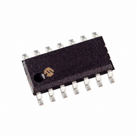
MCP4922-E/SL Microchip Technology, MCP4922-E/SL Datasheet - Page 15

MCP4922-E/SL
Manufacturer Part Number
MCP4922-E/SL
Description
IC DAC 12BIT DUAL W/SPI 14SOIC
Manufacturer
Microchip Technology
Specifications of MCP4922-E/SL
Number Of Converters
2
Package / Case
14-SOIC (3.9mm Width), 14-SOL
Settling Time
4.5µs
Number Of Bits
12
Data Interface
Serial, SPI™
Voltage Supply Source
Single Supply
Operating Temperature
-40°C ~ 125°C
Mounting Type
Surface Mount
Resolution
12 bit
Interface Type
Serial (3-Wire, SPI, Microwire)
Supply Voltage (max)
5.5 V
Supply Voltage (min)
2.7 V
Maximum Operating Temperature
+ 125 C
Mounting Style
SMD/SMT
Minimum Operating Temperature
- 40 C
Lead Free Status / RoHS Status
Lead free / RoHS Compliant
Power Dissipation (max)
-
Lead Free Status / Rohs Status
Lead free / RoHS Compliant
Available stocks
Company
Part Number
Manufacturer
Quantity
Price
Company:
Part Number:
MCP4922-E/SL
Manufacturer:
NMB
Quantity:
2 000
Part Number:
MCP4922-E/SL
Manufacturer:
MICROCHIP/微芯
Quantity:
20 000
3.0
The descriptions of the pins are listed in Table 3-1.
TABLE 3-1:
3.1
V
supply is relative to AV
5.5V. A decoupling capacitor on V
to achieve maximum performance.
3.2
CS is the chip select input, which requires an active-low
signal to enable serial clock and data functions.
3.3
SCK is the SPI compatible serial clock input.
3.4
SDI is the SPI compatible serial data input.
3.5
LDAC (the latch DAC syncronization input) transfers
the input latch registers to the DAC registers (output
latches) when low. Can also be tied low if transfer on
the rising edge of CS is desired.
2004 Microchip Technology Inc.
DD
MCP4921
Pin No.
is the positive power supply input. The input power
—
—
—
—
—
—
1
2
3
4
5
7
6
8
PIN DESCRIPTIONS
Positive Power Supply Input (V
Chip Select (CS)
Serial Clock Input (SCK)
Serial Data Input (SDI)
Latch DAC Input (LDAC)
PIN FUNCTION TABLE
MCP4922
Pin No.
SS
10
12
13
14
11
1
2
3
4
5
6
7
8
9
and can range from 2.7V to
DD
is recommended
Symbol
SHDN
V
V
V
LDAC
V
AV
SCK
V
SDI
NC
NC
NC
OUTB
REFB
OUTA
CS
REFA
DD
SS
DD
)
Positive Power Supply Input (2.7V to 5.5V)
No Connection
Chip Select Input
Serial Clock Input
Serial Data Input
No Connection
No Connection
Syncronization input used to transfer DAC settings from serial
latches to the output latches.
Hardware Shutdown Input
DAC
DAC
Analog ground
DAC
DAC
B
B
A
A
Output
Voltage Input (AV
Voltage Input (AV
Output
3.6
SHDN is the hardware shutdown input that requires an
active-low input signal to configure the DACs in their
low-power Standby mode.
3.7
V
amplifier drives these pins with a range of AV
3.8
V
The analog signal on these pins is utilized to set the ref-
erence voltage on the string DAC. The input signal can
range from AV
3.9
AV
OUTA
REFA
SS
is the analog ground pin.
and V
and V
Hardware Shutdown Input (SHDN)
DAC
DAC
(V
Analog Ground (AV
REFA
OUTB
REFB
SS
SS
SS
x
X
MCP4921/4922
to V
to V
Function
Outputs (V
Voltage Reference Inputs
to V
, V
are DAC outputs. The DAC output
are DAC voltage reference inputs.
DD
DD
REFB
DD
)
)
.
)
OUTA
SS
DS21897A-page 15
, V
)
OUTB
SS
)
to V
DD
.


