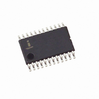
X9400WV24I-2.7T1 Intersil, X9400WV24I-2.7T1 Datasheet - Page 12

X9400WV24I-2.7T1
Manufacturer Part Number
X9400WV24I-2.7T1
Description
IC XDCP QUAD 64-TAP 10K 24-TSSOP
Manufacturer
Intersil
Series
XDCP™r
Datasheet
1.X9400WV24-2.7.pdf
(19 pages)
Specifications of X9400WV24I-2.7T1
Taps
64
Resistance (ohms)
10K
Number Of Circuits
4
Temperature Coefficient
300 ppm/°C Typical
Memory Type
Non-Volatile
Interface
SPI, 3-Wire Serial
Voltage - Supply
2.7 V ~ 5.5 V
Operating Temperature
-40°C ~ 85°C
Mounting Type
Surface Mount
Package / Case
24-TSSOP
Resistance In Ohms
10K
Lead Free Status / RoHS Status
Contains lead / RoHS non-compliant
D.C. OPERATING CHARACTERISTICS (Over the recommended operating conditions unless otherwise specified.)
ENDURANCE AND DATA RETENTION
CAPACITANCE
POWER-UP TIMING
POWER-UP REQUIREMENTS (Power-up sequencing
can affect correct recall of the wiper registers)
The preferred power-on sequence is as follows: First
V
Voltage should not be applied to the potentiometer
pins before V+ or V- is applied. The V
specifi-cation should be met, and any glitches or slope
changes in the V
possible. If V
0.1V for more than 1 second before powering up again
in order for proper wiper register recall. Also, V
should not reverse polarity by more than 0.5V. Recall
of wiper position will not be complete until V
and V-reach their final value.
Symbol
CC
I
I
Symbol
V
C
t
V
CC1
CC2
I
I
V
Symbol
R
SB
I
LO
t
C
t
, then the potentiometer pins, R
LI
OL
OUT
PUW
IH
PUR
IL
IN
V
CC
(4)
(4)
(5)
(5)
Minimum endurance
(4)
V
V
Write)
V
Input leakage current
Output leakage current
Input HIGH voltage
Input LOW voltage
Output LOW voltage
Data retention
CC
CC
CC
CC
Parameter
Output capacitance (SO)
Input capacitance (A0, A1, SI, and SCK)
powers down, it should be held below
supply current (Nonvolatile
supply current (Active)
current (standby)
CC
Power-up to initiation of read operation
Power-up to initiation of write operation
V
CC
line should be held to <100mV if
Parameter
Power-up ramp
12
Parameter
Test
H
, R
CC
L
, and R
ramp rate
V
100,000
CC
Min.
Min.
CC
100
-0.5
x 0.7
, V+
CC
W
.
X9400
Typ.
Limits
EQUIVALENT A.C. LOAD CIRCUIT
V
V
CC
CC
Max.
400
0.4
10
10
Max.
1
1
+ 0.5
x 0.1
8
6
Min.
0.2
Data changes per bit per register
Units
mA
µA
µA
µA
µA
SDA Output
V
V
V
f
Other Inputs = V
f
Other Inputs = V
SCK = SI = V
V
V
I
Unit
SCK
SCK
OL
pF
pF
IN
OUT
years
Max.
Unit
50
= 3mA
1
5
= V
= 2MHz, SO = Open,
= 2MHz, SO = Open,
= V
SS
Test Conditions
SS
5V
to V
1533Ω
100pF
to V
SS
Test Conditions
CC
, Addr. = V
SS
SS
CC
V
V
OUT
IN
V/msec
Unit
ms
ms
= 0V
= 0V
July 28, 2006
SS
FN8189.3


