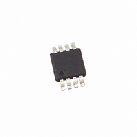
ISL90810WIU8 Intersil, ISL90810WIU8 Datasheet - Page 9

ISL90810WIU8
Manufacturer Part Number
ISL90810WIU8
Description
IC XDCP 256-TAP 10KOHM 8-MSOP
Manufacturer
Intersil
Series
XDCP™r
Datasheet
1.ISL90810UIU8Z-TK.pdf
(11 pages)
Specifications of ISL90810WIU8
Taps
256
Resistance (ohms)
10K
Number Of Circuits
1
Temperature Coefficient
35 ppm/°C Typical
Memory Type
Volatile
Interface
I²C, 2-Wire Serial
Voltage - Supply
2.7 V ~ 5.5 V
Operating Temperature
-40°C ~ 85°C
Mounting Type
Surface Mount
Package / Case
8-MSOP, Micro8™, 8-uMAX, 8-uSOP,
Resistance In Ohms
10K
Lead Free Status / RoHS Status
Contains lead / RoHS non-compliant
Available stocks
Company
Part Number
Manufacturer
Quantity
Price
Company:
Part Number:
ISL90810WIU8Z
Manufacturer:
Intersil
Quantity:
166
The ISL90810 responds with an ACK after recognition of a
START condition followed by a valid Identification Byte, and
once again after successful receipt of an Address Byte. The
ISL90810 also responds with an ACK after receiving a Data
Byte of a write operation. The master must respond with an
ACK after receiving a Data Byte of a read operation.
A valid Identification Byte contains 0101000 as the seven
MSBs. The LSB is the Read/Write bit. Its value is “1” for a
Read operation, and “0” for a Write operation (See Table 1)
The address byte is set to 00h and follows the identification
byte. Read and write operations always point to address
00h, indicating the WR for the device.
Write Operation
A Write operation requires a START condition, followed by a
valid Identification Byte, a valid Address Byte, a Data Byte,
and a STOP condition. After each of the three bytes, the
ISL90810 responds with an ACK. At this time the device
enters its standby state (See Figure 17).
(MSB)
0
TABLE 1. IDENTIFICATION BYTE FORMAT
SDA OUTPUT FROM
SDA OUTPUT FROM
1
TRANSMITTER
SCL FROM
RECEIVER
SDA
0
SCL
MASTER
1
9
START
FIGURE 15. VALID DATA CHANGES, START, AND STOP CONDITIONS
START
0
FIGURE 16. ACKNOWLEDGE RESPONSE FROM RECEIVER
HIGH IMPEDANCE
0
0
1
(LSB)
R/W
STABLE
DATA
ISL90810
CHANGE
DATA
Data Protection
A valid Identification Byte. Address Byte, and total number of
SCL pulses act as a protection for the registers. During a
Write sequence, the Data Byte is loaded into an internal shift
register as it is received. The Data Byte is transferred to the
Wiper Register (WR) at the falling edge of the SCL pulse
that loads the last bit (LSB) of the Data Byte.
Read Operation
A Read operation consists of a three byte instruction
followed by one Data Byte (See Figure 18). The master
initiates the operation issuing the following sequence: a
START, the identification byte with the R/W bit set to "0", an
Address Byte, a second START, and a second Identification
byte with the R/W bit set to "1". After each of the three bytes,
the ISL90810 responds with an ACK. The the ISL90810
transmits Data Bytes as long as the master responds with an
ACK during the SCL cycle following the eighth bit of each
byte. The master terminates the read operation (issuing a
ACK and a STOP condition) following the last bit of the Data
Byte (See Figure 18).
STABLE
DATA
8
HIGH IMPEDANCE
STOP
ACK
9
November 10, 2006
FN8234.2


