X9221WP Intersil, X9221WP Datasheet - Page 2
X9221WP
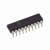
Manufacturer Part Number
X9221WP
Description
IC DCP DUAL 10K 64TP 20DIP
Manufacturer
Intersil
Series
XDCP™r
Datasheet
1.X9221UP.pdf
(15 pages)
Specifications of X9221WP
Taps
64
Resistance (ohms)
10K
Number Of Circuits
2
Temperature Coefficient
30 ppm/°C Typical
Memory Type
Non-Volatile
Interface
I²C, 2-Wire Serial
Voltage - Supply
4.5 V ~ 5.5 V
Operating Temperature
0°C ~ 70°C
Mounting Type
Through Hole
Package / Case
20-DIP (0.300", 7.62mm)
Resistance In Ohms
10K
Lead Free Status / RoHS Status
Contains lead / RoHS non-compliant
Available stocks
Company
Part Number
Manufacturer
Quantity
Price
Company:

Part Number:
X9221WP
Manufacturer:
Intersil
Quantity:
1 500
Part Number:
X9221WP
Manufacturer:
XICOR
Quantity:
20 000


X9221
PIN DESCRIPTIONS
Host Interface Pins
Serial Clock (SCL)
The SCL input is used to clock data into and out of the
X9221.
Serial Data (SDA)
SDA is a bidirectional pin used to transfer data into
and out of the device. It is an open drain output and
may be wire-ORed with any number of open drain or
open collector outputs. An open drain output requires
the use of a pull-up resistor. For selecting typical val-
ues, refer to the guidelines for calculating typical val-
ues on the bus pull-up resistors graph.
Address
The Address inputs are used to set the least signifi-
cant 4 bits of the 8-bit slave address. A match in the
slave address serial data stream must be made with
the Address input in order to initiate communication
with the X9221
Potentiometer Pins
V
The V
minal connections on either end of a mechanical
potentiometer.
V
The wiper outputs are equivalent to the wiper output of
a mechanical potentiometer.
PIN CONFIGURATION
REV 1.1 8/8/02
H
W
/R
/R
H
W
H
(V
/R
(V
H0
H
W0
V
V
/R
V
V
and V
W0
V
W1
V
H1
H0
H0
L0
L1
/R
/R
/R
SDA
/R
/R
V
/R
/R
–V
W0
SS
W0
W1
A0
A2
H1
L0
L0
L1
L
H1
–V
/R
/R
L
W1
1
2
3
4
5
6
7
8
9
10
H1
inputs are equivalent to the ter-
/R
DIP/SOIC
), V
W1
X9221
L
)
/R
L
20
19
18
17
16
15
14
13
12
(V
11
L0
/R
V
RES
RES
RES
A1
A3
SCL
RES
RES
RES
L0
CC
–V
L1
/R
www.xicor.com
L1
)
PIN NAMES
PRINCIPLES OF OPERATION
The X9221 is a highly integrated microcircuit incorpo-
rating two resistor arrays, their associated registers
and counters and the serial interface logic providing
direct communication between the host and the XDCP
potentiometers.
Serial Interface
The X9221 supports a bidirectional bus oriented proto-
col. The protocol defines any device that sends data
onto the bus as a transmitter and the receiving device
as the receiver. The device controlling the transfer is a
master and the device being controlled is the slave.
The master will always initiate data transfers and pro-
vide the clock for both transmit and receive operations.
Therefore, the X9221 will be considered a slave device
in all applications.
Clock and Data Conventions
Data states on the SDA line can change only during
SCL LOW periods (t
SCL HIGH are reserved for indicating start and stop
conditions.
Start Condition
All commands to the X9221 are preceded by the start
condition, which is a HIGH to LOW transition of SDA
while SCL is HIGH (t
monitors the SDA and SCL lines for the start condition,
and will not respond to any command until this condi-
tion is met.
Stop Condition
All communications must be terminated by a stop con-
dition, which is a LOW to HIGH transition of SDA while
SCL is HIGH.
SCL
SDA
A0–A3
V
V
V
RES
H0
L0
W0
/R
/R
/R
H0
H0
Symbol
W0
–V
–V
–V
L1
H1
W1
/R
/R
/R
L0
H1
Characteristics subject to change without notice.
W1
,
LOW
HIGH
Serial Clock
Serial Data
Address
Potentiometers
(terminal equivalent)
Potentiometers
(wiper equivalent)
Reserved (Do not connect)
). SDA state changes during
). The X9221 continuously
Description
2 of 15
Related parts for X9221WP
Image
Part Number
Description
Manufacturer
Datasheet
Request
R

Part Number:
Description:
Intersil Corporation [CMOS Serial Controller Interface]
Manufacturer:
Intersil Corporation
Datasheet:
Part Number:
Description:
Manufacturer:
Intersil Corporation
Datasheet:
Part Number:
Description:
357-036-542-201 CARDEDGE 36POS DL .156 BLK LOPRO
Manufacturer:
Intersil Corporation
Datasheet:
Part Number:
Description:
1024-Word x 4-Bit LSI Static RAM
Manufacturer:
Intersil Corporation
Datasheet:
Part Number:
Description:
General Purpose NPN Transistor Arrays FN341.4
Manufacturer:
Intersil Corporation
Datasheet:
Part Number:
Description:
CMOS 16-Bit Microprocessor
Manufacturer:
Intersil Corporation
Datasheet:
Part Number:
Description:
Manufacturer:
Intersil Corporation
Datasheet:
Part Number:
Description:
Manufacturer:
Intersil Corporation
Datasheet:
Part Number:
Description:
Manufacturer:
Intersil Corporation
Datasheet:
Part Number:
Description:
Manufacturer:
Intersil Corporation
Datasheet:
Part Number:
Description:
CMOS 6-Bit Latch and Decoder Memory Interfaces
Manufacturer:
Intersil Corporation
Datasheet:
Part Number:
Description:
CA3046General Purpose NPN Transistor Arrays
Manufacturer:
Intersil Corporation
Datasheet:
Part Number:
Description:
Manufacturer:
Intersil Corporation
Datasheet:
Part Number:
Description:
TR909 DLC/FLC SLIC with Low Power Standby
Manufacturer:
Intersil Corporation
Datasheet:
Part Number:
Description:
Manufacturer:
Intersil Corporation
Datasheet: