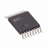
DS1858E-050+ Maxim Integrated Products, DS1858E-050+ Datasheet - Page 11

DS1858E-050+
Manufacturer Part Number
DS1858E-050+
Description
IC RES TEMP 50/50K 3MON 16-TSSOP
Manufacturer
Maxim Integrated Products
Datasheet
1.DS1858E-050.pdf
(22 pages)
Specifications of DS1858E-050+
Taps
256
Resistance (ohms)
50K
Number Of Circuits
2
Temperature Coefficient
50 ppm/°C Typical
Memory Type
Non-Volatile
Interface
I²C, 2-Wire Serial
Voltage - Supply
3 V ~ 5.5 V
Operating Temperature
-40°C ~ 95°C
Mounting Type
Surface Mount
Package / Case
16-TSSOP
Resistance In Ohms
50K
Lead Free Status / RoHS Status
Lead free / RoHS Compliant
The value of each variable resistor is determined by
a temperature-addressed look-up table, which can
assign a unique value (00h to FFh) to each resistor for
every 2°C increment over the -40°C to +102°C range
(see Table 3). See the Temperature Conversion section
for more information.
The variable resistors can also be used in manual
mode. If the TEN bit equals 0, then the resistors are in
manual mode and the temperature indexing is dis-
abled. The user sets the resistors in manual mode by
writing to addresses 82h and 83h in Table 01 to control
resistors 0 and 1, respectively.
Main and auxiliary memories can be accessed by two
separate device addresses. The Main Device address
is A2h (or value in Table 01 byte 8Ch, when ADFIX = 1)
and the Auxiliary Device address is A0h. A user option
is provided to respond to one or two device addresses.
This feature can be used to save component count in
SFF applications (Main Device address can be used)
or other applications where both GBIC (Auxiliary
Device address can be used) and monitoring functions
are implemented and two device addresses are need-
ed. The memory blocks are enabled with the corre-
sponding device address. Memory space from 80h and
up is accessible only through the Main Device address.
This memory is organized as three tables; the desired
table can be selected by the contents of memory loca-
tion 7Fh, Main Device. The Auxiliary Device address
has no access to the tables, but the Auxiliary Device
address can be mapped into the Main Device’s memo-
ry space as a fourth table. Device addresses are pro-
grammable with two control bits in EEPROM.
ADEN configures memory access to respond to differ-
ent device addresses (see Tables 4 and 5).
The default device address for EEPROM-generated
addresses is A2h.
If the ADEN bit is 1, additional 128 bytes of EEPROM
are accessible through the Main Device, selected as
Table 00 (see Figure 3). In this configuration, the
Auxiliary Device is not accessible. APEN controls the
protection of Table 00 regardless of the setting of
ADEN.
ADFIX (address fixed) determines whether the Main
Device address is determined by an EEPROM byte
(Table 01, byte 8Ch, when ADFIX =1). There can be up
to 128 devices sharing a common 2-wire bus, with
each device having its own unique device address.
Memory Description
Variable Resistors
____________________________________________________________________
Resistors with Three Monitors
Dual Temperature-Controlled
Memory access from either device address can be
either read/write or read only. Write protection
is accomplished by a combination of control bits in
EEPROM (APEN and MPEN in configuration register
89h) and a write-protect enable (WPEN) pin. Since the
WPEN pin is often not accessible from outside the mod-
ule, this scheme effectively allows the module to be
locked by the manufacturer to prevent accidental writes
by the end user.
Separate write protection is provided for the Auxiliary
and Main Device address through distinct bits APEN
and MPEN. APEN and MPEN are bits from configura-
tion register 89h, Table 01. Due to the location, the
APEN and MPEN bits can only be written through the
Main Device address. The control of write privileges
through the Auxiliary Device address is dependent on
the value of APEN. Care should be taken with the set-
ting of MPEN, once set to a 1, assuming WPEN is high,
access through the Main Device is thereafter denied
unless WPEN is taken to a low level. By this means
inadvertent end-user write access can be denied.
Main Device address space 60h to 7Fh is SRAM and is
not write protected by APEN, MPEN, or WPEN. For
example, the user may reset flags set by the device.
Bytes designated as “Reserved” may be used as
scratchpad, but they will not be stored in a power cycle
because of their volatility. These bytes are reserved for
added functionality in future versions of this device.
Note that in single device mode (ADEN bit = 1), APEN
determines the protection level of Table 00, indepen-
dent of WPEN.
The write-protect operation, for both Main and Auxiliary
Devices, is summarized in Tables 6 and 7.
Table 6. Main Device
Table 7. Auxiliary Device
WPEN
APEN
X
0
1
0
1
WPEN
X
X
MPEN
X
0
1
PROTECT AUXILIARY
Memory Protection
PROTECT MAIN
Yes
No
Yes
No
No
11


