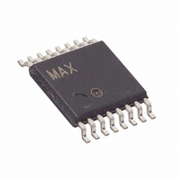
DS1856E-020+ Maxim Integrated Products, DS1856E-020+ Datasheet - Page 27

DS1856E-020+
Manufacturer Part Number
DS1856E-020+
Description
IC RES TEMP-CNTRL 20/20K 16TSSOP
Manufacturer
Maxim Integrated Products
Datasheet
1.DS1856B-050.pdf
(31 pages)
Specifications of DS1856E-020+
Taps
256
Resistance (ohms)
20K
Number Of Circuits
2
Temperature Coefficient
50 ppm/°C Typical
Memory Type
Non-Volatile
Interface
I²C, 2-Wire Serial
Voltage - Supply
2.85 V ~ 5.5 V
Operating Temperature
-40°C ~ 95°C
Mounting Type
Surface Mount
Package / Case
16-TSSOP
Resistance In Ohms
20K
Lead Free Status / RoHS Status
Lead free / RoHS Compliant
During power-up, the device is inactive until V
exceeds the digital power-on-reset voltage (POD). At this
voltage, the digital circuitry, which includes the 2-wire
interface, becomes functional. However, EEPROM-
backed registers/settings cannot be internally read
(recalled into shadow SRAM) until V
log power-on-reset voltage (POA), at which time the
remainder of the device becomes fully functional. Once
V
Device memory is timed to go from a 1 to a 0 and indi-
cates when analog-to-digital conversions begin. If V
ever dips below POA, the RDYB bit reads as a 1 again.
Once a device exceeds POA and the EEPROM is
recalled, the values remain active (recalled) until V
below POD.
For 2-wire device addresses sourced from EEPROM
(ADFIX = 1), the device address defaults to A2h until V
exceeds POA and the EEPROM values are recalled. The
Auxiliary Device (A0h) is always available within this volt-
age window (between POD and the EEPROM recall)
regardless of the programmed state of ADEN.
Furthermore, as the device powers up, the V
flag (bit 4 of 70h in Main Device) defaults to a 1 until the
first V
clears the flag accordingly.
Clock and Data Transitions: The SDA pin is normally
pulled high with an external resistor or device. Data on
the SDA pin may only change during SCL-low time
periods. Data changes during SCL-high periods will
indicate a START or STOP condition depending on the
conditions discussed below. See the timing diagrams
in Figures 5 and 6 for further details.
START Condition: A high-to-low transition of SDA with
SCL high is a START condition that must precede any
other command. See the timing diagrams in Figures 5
and 6 for further details.
STOP Condition: A low-to-high transition of SDA with
SCL high is a STOP condition. After a read or write
sequence, the stop command places the DS1856 into a
low-power mode. See the timing diagrams in Figures 5
and 6 for further details.
Acknowledge: All address and data bytes are trans-
mitted through a serial protocol. The DS1856 pulls the
SDA line low during the ninth clock pulse to acknowl-
edge that it has received each word.
nally Calibrated Monitors and Password Protection
CC
Dual, Temperature-Controlled Resistors with Inter-
exceeds POA, the RDYB bit in byte 6Eh of the Main
CC
Power-Up and Low-Voltage Operation
analog-to-digital conversion occurs and sets or
2-Wire Operation
CC
____________________________________________________________________
exceeds the ana-
CC
lo alarm
CC
falls
CC
CC
CC
Standby Mode: The DS1856 features a low-power
mode that is automatically enabled after power-on,
after a STOP command, and after the completion of all
internal operations.
Device Addressing: The DS1856 must receive an 8-bit
device address, the slave address byte, following a
START condition to enable a specific device for a read
or write operation. The address is clocked into this part
MSB to LSB. The address byte consists of either A2h or
the value in Table 03, 8Ch for the Main Device or A0h
for the Auxiliary Device, then the
must match the address programmed into Table 03,
8Ch or A0h (for the Auxiliary Device). If a device
address match occurs, this part will output a zero for
one clock cycle as an acknowledge and the corre-
sponding block of memory is enabled (see the Memory
Organization section). If the R/W bit is high, a read
operation is initiated. If the R/W is low, a write operation
is initiated (see the Memory Organization section). If the
address does not match, this part returns to a low-
power mode.
After receiving a matching address byte with the R/W
bit set low, if there is no write protect, the device goes
into the write mode of operation (see the Memory
Organization section). The master must transmit an 8-
bit EEPROM memory address to the device to define
the address where the data is to be written. After the
byte has been received, the DS1856 transmits a zero
for one clock cycle to acknowledge the address has
been received. The master must then transmit an 8-bit
data word to be written into this address. The DS1856
again transmits a zero for one clock cycle to acknowl-
edge the receipt of the data. At this point, the master
must terminate the write operation with a STOP condi-
tion. The DS1856 then enters an internally timed write
process t
abled during this byte write cycle.
The DS1856 is capable of an 8-byte page write. A page
is any 8-byte block of memory starting with an address
evenly divisible by eight and ending with the starting
address plus seven. For example, addresses 00h
through 07h constitute one page. Other pages would
be addresses 08h through 0Fh, 10h through 17h, 18h
through 1Fh, etc.
w
to the EEPROM memory. All inputs are dis-
Write Operations
R/W bit. This byte
Page Write
27


