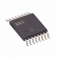
DS1847E-050+T&R Maxim Integrated Products, DS1847E-050+T&R Datasheet - Page 9

DS1847E-050+T&R
Manufacturer Part Number
DS1847E-050+T&R
Description
IC RES TEMP-CNTRL 50/10K 16TSSOP
Manufacturer
Maxim Integrated Products
Datasheet
1.DS1847E-050.pdf
(17 pages)
Specifications of DS1847E-050+T&R
Taps
256
Resistance (ohms)
10K, 50K
Number Of Circuits
2
Temperature Coefficient
850 ppm/°C Typical
Memory Type
Non-Volatile
Interface
I²C, 2-Wire Serial
Voltage - Supply
3 V ~ 5.5 V
Operating Temperature
-40°C ~ 95°C
Mounting Type
Surface Mount
Package / Case
16-TSSOP
Resistance In Ohms
10K and 50K
Lead Free Status / RoHS Status
Lead free / RoHS Compliant
DS1847
The master must terminate the write cycle with a STOP condition or the data clocked into the DS1847
will not be latched into permanent memory.
Acknowledge Polling: Once the internally-timed write has started and the DS1847 inputs are disabled,
acknowledge polling can be initiated. The process involves transmitting a START condition followed by
the device address. The R/W bit signifies the type of operation that is desired. The read or write sequence
will only be allowed to proceed if the internal write cycle has completed and the DS1847 responds with a
zero.
Read Operations: After receiving a matching address byte with the R/W bit set high, the device goes
into the read mode of operation. There are three read operations: current address read, random read, and
sequential address read.
CURRENT ADDRESS READ
The DS1847 has an internal address register that maintains the address used during the last read or write
operation, incremented by one. This data is maintained as long as V
is valid. If the most recent address
CC
was the last byte in memory, then the register resets to the first address. This address stays valid between
operations as long as power is available.
Once the device address is clocked in and acknowledged by the DS1847 with the R/W bit set to high, the
current address data word is clocked out. The master does not respond with a zero, but does generate a
STOP condition afterwards.
RANDOM READ
A random read requires a dummy byte write sequence to load in the data word address. Once the device
and data address bytes are clocked in by the master and acknowledged by the DS1847, the master must
generate another START condition. The master now initiates a current address read by sending the device
address with the read/write bit set high. The DS1847 will acknowledge the device address and serially
clocks out the data byte.
SEQUENTIAL ADDRESS READ
Sequential reads are initiated by either a current address read or a random address read. After the master
receives the first data byte, the master responds with an acknowledge. As long as the DS1847 receives
this acknowledge after a byte is read, the master may clock out additional data words from the DS1847.
After reaching address FFh, it resets to address 00h.
The sequential read operation is terminated when the master initiates a stop condition. The master does
not respond with a zero.
For a more detailed description of 2-wire theory of operation, refer to the next section.
9 of 17


