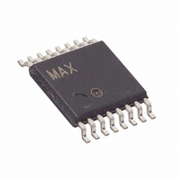
DS1847E-050+T&R Maxim Integrated Products, DS1847E-050+T&R Datasheet - Page 11

DS1847E-050+T&R
Manufacturer Part Number
DS1847E-050+T&R
Description
IC RES TEMP-CNTRL 50/10K 16TSSOP
Manufacturer
Maxim Integrated Products
Datasheet
1.DS1847E-050.pdf
(17 pages)
Specifications of DS1847E-050+T&R
Taps
256
Resistance (ohms)
10K, 50K
Number Of Circuits
2
Temperature Coefficient
850 ppm/°C Typical
Memory Type
Non-Volatile
Interface
I²C, 2-Wire Serial
Voltage - Supply
3 V ~ 5.5 V
Operating Temperature
-40°C ~ 95°C
Mounting Type
Surface Mount
Package / Case
16-TSSOP
Resistance In Ohms
10K and 50K
Lead Free Status / RoHS Status
Lead free / RoHS Compliant
slave by not generating an acknowledge bit on the last byte that has been clocked out of the slave. In this
case, the slave must leave the data line HIGH to enable the master to generate the STOP condition.
1. Data transfer from a master transmitter to a slave receiver. The first byte transmitted by the master is
2. Data transfer from a slave transmitter to a master receiver. The master transmits the first byte (the
The master device generates all serial clock pulses and the START and STOP conditions. A transfer is
ended with a STOP condition or with a repeated START condition. Since a repeated START condition is
also the beginning of the next serial transfer, the bus will not be released.
The DS1847 may operate in the following two modes:
1. Slave receiver mode: Serial data and clock are received through SDA and SCL, respectively. After
2. Slave transmitter mode: The first byte is received and handled as in the slave receiver mode.
3. Slave Address: Command/control byte is the first byte received following the START condition from
Following the START condition, the DS1847 monitors the SDA bus checking the device type identifier
being transmitted. Upon receiving the 1010 control code, the appropriate device address bits, and the
read/write bit, the slave device outputs an acknowledge signal on the SDA line.
WRITE PROTECT
The write-protect input pin (WP) protects all memory (including EEPROM), control registers, and look-
up tables from alteration in an application.
temperature/resistor updates. If set to a logic 0, the device is not write protected and can be written to via
the 2-wire interface. This pin has an internal pull-up resistor.
the command/control byte. Next follows a number of data bytes. The slave returns an acknowledge bit
after each received byte.
command/control byte) to the slave. The slave then returns an acknowledge bit. Next, follows a
number of data bytes transmitted by the slave to the master. The master returns an acknowledge bit
after all received bytes other than the last byte. At the end of the last received byte, a ‘not
acknowledge’ can be returned.
each byte is received, an acknowledge bit is transmitted. START and STOP conditions are recognized
as the beginning and end of a serial transfer. Address recognition is performed by hardware after
reception of the slave (device) address and direction bit.
However, in this mode the direction bit will indicate that the transfer direction is reversed. Serial data
is transmitted on SDA by the DS1847, while the serial clock is input on SCL. START and STOP
conditions are recognized as the beginning and end of a serial transfer.
the master device. The command/control byte consists of a 4-bit control code. For the DS1847, this is
set as 1010 binary for read/write operations. The next 3 bits of the command/ control byte are the
device select bits or slave address (A2, A1, A0). They are used by the master device to select which
of eight devices is to be accessed. When reading or writing the DS1847, the device-select bits must
match the device-select pins (A2, A1, A0). The last bit of the command/control byte (R/W) defines
the operation to be performed. When set to a 1, a read operation is selected, and when set to a 0, a
write operation is selected.
11 of 17
However, this does not interfere with internal


