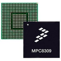
MPC8309VMAHFCA Freescale Semiconductor, MPC8309VMAHFCA Datasheet - Page 66

MPC8309VMAHFCA
Manufacturer Part Number
MPC8309VMAHFCA
Description
417/333/233 MP Std Tmp
Manufacturer
Freescale Semiconductor
Datasheet
1.MPC8309VMAHFCA.pdf
(81 pages)
Specifications of MPC8309VMAHFCA
Processor Series
MPC8309
Core
e300c3
Data Bus Width
32 bit
Data Ram Size
512 MB
Interface Type
USB, CAN, UART, PCI
Maximum Clock Frequency
417 MHz
Number Of Programmable I/os
56
Operating Supply Voltage
- 0.3 V to + 1.26 V
Maximum Operating Temperature
+ 105 C
Mounting Style
SMD/SMT
Operating Temperature Range
0 C to + 105 C
Processor To Be Evaluated
MPC8309
Supply Current (max)
5 uA
Lead Free Status / Rohs Status
Details
Available stocks
Company
Part Number
Manufacturer
Quantity
Price
Company:
Part Number:
MPC8309VMAHFCA
Manufacturer:
Freescale Semiconductor
Quantity:
10 000
Clocking
23.1
When the MPC8309 is configured as a PCI host device (RCWH[PCIHOST] = 1), SYS_CLK_IN is its
primary input clock. SYS_CLK_IN feeds the PCI clock divider (2) and the PCI_SYNC_OUT and
PCI_CLK multiplexors. The CFG_CLKIN_DIV configuration input selects whether SYS_CLK_IN or
SYS_CLK_IN/2 is driven out on the PCI_SYNC_OUT signal.
PCI_SYNC_OUT is connected externally to PCI_SYNC_IN to allow the internal clock subsystem to
synchronize to the system PCI clocks. PCI_SYNC_OUT must be connected properly to PCI_SYNC_IN,
with equal delay to all PCI agent devices in the system.
23.1.1
When the MPC8309 is configured as a PCI host, it provides three separate clock output signals,
PCI_CLK[0:2], for external PCI agents.
When the device comes out of reset, the PCI clock outputs are disabled and are actively driven to a steady
low state. Each of the individual clock outputs can be enabled (enable toggling of the clock) by setting its
corresponding OCCR[PCICOEn] bit. All output clocks are phase-aligned to each other.
23.2
When the MPC8309 is configured as a PCI agent device, PCI_SYNC_IN is the primary input clock. In
agent mode, the SYS_CLK_IN signal should be tied to GND, and the clock output signals, PCI_CLKn and
PCI_SYNC_OUT, are not used.
23.3
As shown in
(PLL) and the clock unit to create four major clock domains:
The csb_clk frequency is derived from the following equation:
In PCI host mode,
The csb_clk serves as the clock input to the e300 core. A second PLL inside the core multiplies up the
csb_clk frequency to create the internal clock for the core (core_clk). The system and core PLL multipliers
are selected by the SPMF and COREPLL fields in the reset configuration word low (RCWL) which is
loaded at power-on reset or by one of the hard-coded reset options. For more information, see the Reset
66
•
•
•
•
MPC8309 PowerQUICC II Pro Integrated Communications Processor Family Hardware Specifications, Rev. 1
The coherent system bus clock (csb_clk)
The QUICC Engine clock (qe_clk)
The internal clock for the DDR controller (ddr_clk)
The internal clock for the local bus controller (lbc_clk)
Clocking in PCI Host Mode
Clocking in PCI Agent Mode
System Clock Domains
PCI Clock Outputs (PCI_CLK[0:2])
Figure
csb_clk = [PCI_SYNC_IN × (1 + ~CFG_CLKIN_DIV)] × SPMF
, the primary clock input (frequency) is multiplied up by the system phase-locked loop
PCI_SYNC_IN = SYS_CLK_IN
(1 + ~
CFG_CLKIN_DIV
) .
Freescale Semiconductor
Eqn. 1
Eqn. 2


