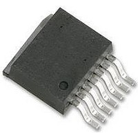
LMZ23603TZ National Semiconductor, LMZ23603TZ Datasheet - Page 17

LMZ23603TZ
Manufacturer Part Number
LMZ23603TZ
Description
POWER MODULE, 36V, 3A, 7TO-PMOD
Manufacturer
National Semiconductor
Datasheet
1.LMZ23603TZ.pdf
(22 pages)
Specifications of LMZ23603TZ
Primary Input Voltage
36V
No. Of Outputs
1
Output Voltage
6V
Output Current
3A
Voltage Regulator Case Style
TO-PMOD
No. Of Pins
7
Operating Temperature Range
-40°C To +125°C
Rohs Compliant
Yes
Available stocks
Company
Part Number
Manufacturer
Quantity
Price
4. Make input and output bus connections as wide as
possible.
This reduces any voltage drops on the input or output of the
converter and maximizes efficiency. To optimize voltage ac-
curacy at the load, ensure that a separate feedback voltage
sense trace is made to the load. Doing so will correct for volt-
age drops and provide optimum output accuracy.
5. Provide adequate device heat-sinking.
Use an array of heat-sinking vias to connect the exposed pad
to the ground plane on the bottom PCB layer. If the PCB has
a plurality of copper layers, these thermal vias can also be
employed to make connection to inner layer heat-spreading
ground planes. For best results use a 6 x 10 via array with
minimum via diameter of 10mils (254 μm) thermal vias spaced
59mils (1.5 mm). Ensure enough copper area is used for heat-
sinking to keep the junction temperature below 125°C.
Additional Features
SYNCHRONIZATION INPUT
The PWM switching frequency can be synchronized to an ex-
ternal frequency source. If this feature is not used, connect
this input either directly to ground, or connect to ground
through a resistor of 1.5 kΩ ohm or less. The allowed syn-
chronization frequency range is 650kHz to 950 kHz. The
typical input threshold is 1.4V transition level. Ideally the input
clock should overdrive the threshold by a factor of 2, so direct
drive from 3.3V logic via a 1.5kΩ Thevenin source resistance
is recommended. Note that applying a sustained “logic 1” cor-
responds to zero Hz PWM frequency and will cause the
module to stop switching.
OUTPUT OVER-VOLTAGE PROTECTION
If the voltage at FB is greater than a 0.86V internal reference,
the output of the error amplifier is pulled toward ground, caus-
ing V
CURRENT LIMIT
The LMZ23603 is protected by both low side (LS) and high
side (HS) current limit circuitry. The LS current limit detection
is carried out during the off-time by monitoring the current
through the LS synchronous MOSFET. Referring to the Func-
tional Block Diagram, when the top MOSFET is turned off, the
inductor current flows through the load, the PGND pin and the
internal synchronous MOSFET. If this current exceeds the
low side current limit level the current limit comparator dis-
ables the start of the next switching period. Switching cycles
are prohibited until current drops below the limit. It should also
be noted that d.c. current limit is dependent on both duty cycle
and temperature as illustrated in the graphs in the typical per-
formance section. The HS current limit monitors the current
of top side MOSFET. Once HS current limit is detected, the
HS MOSFET is shutoff immediately, until the next cycle. Ex-
ceeding HS current limit causes V
exceeding LS current limit is that f
erating frequency.
THERMAL PROTECTION
The junction temperature of the LMZ23603 should not be al-
lowed to exceed its maximum ratings. Thermal protection is
implemented by an internal Thermal Shutdown circuit which
activates at 165 °C (typ) causing the device to enter a low
power standby state. In this state the main MOSFET remains
off causing V
discharged to ground. Thermal protection helps prevent
catastrophic failures for accidental device overheating. When
O
to fall.
O
to fall, and additionally the C
O
SW
to fall. Typical behavior of
drops to 1/2 of the op-
SS
capacitor is
17
the junction temperature falls back below 150 °C (typ Hyst =
15°C) the SS pin is released, V
operation resumes.
Applications requiring maximum output current especially
those at high input voltage may require additional derating at
elevated temperatures.
PRE-BIASED STARTUP
The LMZ23603 will properly start up into a pre-biased output.
This startup situation is common in multiple rail logic applica-
tions where current paths may exist between different power
rails during the startup sequence. The following scope cap-
ture shows proper behavior in this mode. Trace one is Enable
going high. Trace two is 1.5V pre-bias rising to 3.3V. Risetime
determined by C
DISCONTINUOUS CONDUCTION AND CONTINUOUS
CONDUCTION MODES
At light load the regulator will operate in discontinuous con-
duction mode (DCM). With load currents above the critical
conduction point, it will operate in continuous conduction
mode (CCM). In CCM, current flows through the inductor
through the entire switching cycle and never falls to zero dur-
ing the off-time. When operating in DCM, inductor current is
maintained to an average value equaling Iout. Inductor cur-
rent exhibits normal behavior for the emulated current mode
control method used. Output voltage ripple typically increases
during this mode of operation.
Following is a comparison pair of waveforms of the showing
both CCM (upper) and DCM operating modes.
SS
, trace three.
Pre-Biased Startup
O
rises smoothly, and normal
30152625
www.national.com


