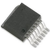
LMZ23603TZ National Semiconductor, LMZ23603TZ Datasheet - Page 15

LMZ23603TZ
Manufacturer Part Number
LMZ23603TZ
Description
POWER MODULE, 36V, 3A, 7TO-PMOD
Manufacturer
National Semiconductor
Datasheet
1.LMZ23603TZ.pdf
(22 pages)
Specifications of LMZ23603TZ
Primary Input Voltage
36V
No. Of Outputs
1
Output Voltage
6V
Output Current
3A
Voltage Regulator Case Style
TO-PMOD
No. Of Pins
7
Operating Temperature Range
-40°C To +125°C
Rohs Compliant
Yes
Available stocks
Company
Part Number
Manufacturer
Quantity
Price
OUTPUT VOLTAGE SELECTION
Output voltage is determined by a divider of two resistors
connected between V
vider is connected to the FB input.
The regulated output voltage determined by the external di-
vider resistors R
V
Rearranging terms; the ratio of the feedback resistors for a
desired output voltage is:
R
These resistors should generally be chosen from values in the
range of 1.0 kΩ to 10.0 kΩ.
For V
rectly and R
output load.
A table of values for R
plified applications schematic on page 2.
SOFT-START CAPACITOR SELECTION
Programmable soft-start permits the regulator to slowly ramp
to its steady state operating point after being enabled, thereby
reducing current inrush from the input supply and slowing the
output voltage rise-time.
Upon turn-on, after all UVLO conditions have been passed,
an internal 1.6mSec circuit slowly ramps the SS/TRK input to
implement internal soft start. If 1.6mSec is an adequate turn–
on time then the Css capacitor can be left unpopulated.
Longer soft-start periods are achieved by adding an external
capacitor to this input.
Soft start duration is given by the formula:
t
This equation can be rearranged as follows:
C
Using a 0.22μF capacitor results in 3.5 msec typical soft-start
duration; and 0.47μF results in 7.5 msec typical. 0.47 μF is a
recommended initial value.
As the soft-start input exceeds 0.796V the output of the power
stage will be in regulation and the 50 μA current is deactivat-
ed. Note that the following conditions will reset the soft-start
capacitor by discharging the SS input to ground with an in-
ternal current sink.
• The Enable input being pulled low
• Thermal shutdown condition
• Internal Vcc UVLO (Approx 4.3V input to V
SS
O
FBT
SS
= 0.796V * (1 + R
= V
= t
/ R
O
REF
SS
= 0.8V the FB pin can be connected to the output di-
FBB
* 50μA / 0.796V (5)
* C
= (V
FBB
SS
FBT
O
can be set to 8.06kΩ to provide minimum
/ Iss = 0.796V * C
/ 0.796V) - 1 (3)
Enable input detail
and R
FBT
O
FBT
and ground. The midpoint of the di-
/ R
Figure 1
FBB
, and R
FBB
is:
) (2)
FBB
SS
, is included in the sim-
/ 50uA (4)
IN
)
30152609
15
TRACKING SUPPLY DIVIDER OPTION
The tracking function allows the module to be connected as
a slave supply to a primary voltage rail (often the 3.3V system
rail) where the slave module output voltage is lower than that
of the master. Proper configuration allows the slave rail to
power up coincident with the master rail such that the voltage
difference between the rails during ramp-up is small (i.e.
<0.15V typ). The values for the tracking resistive divider
should be selected such that the presence of the internal
50uA current source is minimized. In most cases the ratio of
the tracking divider resistors is the same as the ratio of the
output voltage setting divider. Proper operation in tracking
mode dictates the soft-start time of the slave rail be shorter
than the master rail; a condition that is easy satisfy since the
C
supported for the power up interval of the master supply; once
the SS/TRK rises past 0.8V the input is no longer enabled and
the 50 uA internal current source is switched off.
C
None of the required C
in the module. A minimum value of 200 μF is required based
on the values of internal compensation in the error amplifier.
Low ESR tantalum, organic semiconductor or specialty poly-
mer capacitor types are recommended for obtaining lowest
ripple. The output capacitor C
pacitors in parallel placed in close proximity to the module.
The output capacitor assembly must also meet the worst case
minimum ripple current rating of 0.5 * I
equation (14) below. Beyond that, additional capacitance will
reduce output ripple so long as the ESR is low enough to per-
mit it. Loop response verification is also valuable to confirm
closed loop behavior. R
tion schematic and evaluation board for this purpose. It is not
required in the end design.
For applications with dynamic load steps; the following equa-
tion provides a good first pass approximation of C
transient requirements. Where V
output design.
C
Solving:
C
125μF (7)
Note that the stability requirement for 200 µF minimum output
capacitance will take precedence.
One recommended output capacitor combination is a 220uF,
7 milliohm ESR specialty polymer cap in parallel with a 100
SS
O
O
O
≥
≥
SELECTION
I
cap is replaced by R
O-Tran
2.5A / ((0.1V – .007*2.5A) * ( 800000 Hz / 3.3V)
/((*V
O-Tran
Tracking option input detail
– ESR * I
O
LRA
output capacitance is contained with-
Figure 2
TKB
is included on the typical applica-
O–Tran
. The tracking function is only
O
may consist of several ca-
O-Tran
) * ( F*
LR P-P
is 100 mV on a 3.3V
SW
, as calculated in
/ V
O
))(6)
www.national.com
30152615
O
for load
≥


