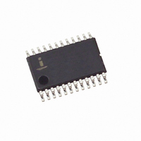
X9408WV24IZ-2.7T1 Intersil, X9408WV24IZ-2.7T1 Datasheet - Page 9

X9408WV24IZ-2.7T1
Manufacturer Part Number
X9408WV24IZ-2.7T1
Description
IC POT DGTL QUAD 10K OHM 24TSSOP
Manufacturer
Intersil
Series
XDCP™r
Datasheet
1.X9408WS24I.pdf
(20 pages)
Specifications of X9408WV24IZ-2.7T1
Taps
64
Resistance (ohms)
10K
Number Of Circuits
4
Temperature Coefficient
300 ppm/°C Typical
Memory Type
Non-Volatile
Interface
I²C, 2-Wire Serial
Voltage - Supply
2.7 V ~ 5.5 V
Operating Temperature
-40°C ~ 85°C
Mounting Type
Surface Mount
Package / Case
24-TSSOP
Resistance In Ohms
10K
Lead Free Status / RoHS Status
Lead free / RoHS Compliant
Other names
X9408WV24IZ-2.7T1TR
TABLE 3.
Instruction Format
NOTES:
Read Wiper Counter Register (WCR)
Write Wiper Counter Register (WCR)
Read Data Register (DR)
Write Data Register (DR)
XFR Data Register (DR) to Wiper Counter Register (WCR)
1. “MACK”/”SACK”: stands for the acknowledge sent by the master/slave.
2. “A3 ~ A0”: stands for the device addresses sent by the master.
3. “X”: indicates that it is a “0” for testing purpose but physically it is a “don’t care” condition.
4. “I”: stands for the increment operation, SDA held high during
5. “D”: stands for the decrement operation, SDA held low during active SCL phase (high).
A
R
A
R
S
T
T
S
T
T
A
R
A
R
(MSB)
S
T
T
S
T
T
S
T
A
R
T
WP5
active SCL phase (high).
V
DEVICE TYPE
0
DEVICE TYPE
0
IDENTIFIER
0
0
DEVICE TYPE
IDENTIFIER
DEVICE TYPE
IDENTIFIER
IDENTIFIER
0
1
1
1
1
DEVICE TYPE
IDENTIFIER
WP4
0
WIPER COUNTER REGISTER, (6-BIT), VOLATILE
0
V
1
0
0
1
1
1
1
A3 A2 A1 A0
0
ADDRESSES
A3
WP3
A3 A2 A1 A0
A3 A2 A1 A0
ADDRESSES
DEVICE
V
ADDRESSES
ADDRESSES
1
DEVICE
A2
DEVICE
DEVICE
9
A1
A3
WP2
V
A0
ADDRESSES
S
A
C
K
A2
DEVICE
S
A
C
K
S
A
C
K
S
A
C
K
1
INSTRUCTION
WP1
V
OPCODE
A1
1
INSTRUCTION
1
1
1
INSTRUCTION
INSTRUCTION
OPCODE
OPCODE
0
OPCODE
0
0
A0
0
(LSB)
WP0
0
V
0
1
1
A
C
K
S
1
R1 R0 P1 P0
DR AND WCR
ADDRESSES
1
X9408
0
0
ADDRESSES
1
R1
0
ADDRESSES
DR AND WCR
ADDRESSES
0
WCR
INSTRUCTION
One 6-bit Wiper Counter Register for each XDCP. (Four 6-bit
registers in total.)
{D5~D0}: These bits specify the wiper position of the
respective XDCP. The Wiper Counter Register is loaded on
power-up by the value in Data Register 0. The contents of
the WCR can be loaded from any of the other Data Register
or directly. The contents of the WCR can be saved in a DR.
R0
0
WCR
OPCODE
1
P1
P1 P0
P1
A
C
K
S
P0
0
P0
0
S
A
C
K
(SENT BY MASTER ON SDA)
S
A
C
K
WIPER POSITION/DATA
0
1
S
A
C
K
0
P5
0
W
0
(SENT BY SLAVE ON SDA)
0
(SENT BY MASTER ON SDA)
R1
P4
0
W
(SENT BY SLAVE ON SDA)
0
WIPER POSITION/DATA
WP
WIPER POSITION
5
WIPER POSITION
DR AND WCR
P5
ADDRESSES
W
P3
W
P5
W
R0
WP
4
P4
P2
W
W
P4
W
WP
P1
3
P3
P1
W
W
P3
W
WP
P0
P2
W
2
W
P2
W
P0
WP
S
A
C
K
P1
W
1
P1
W
January 15, 2009
O
S
T
P
WP
P0
W
S
A
C
K
P0
0
W
FN8191.4
S
A
C
K
M
A
C
K
M
A
C
K
HIGH-VOLTAGE
O
WRITE CYCLE
S
T
P
O
S
O
P
S
P
T
T
O
S
T
P


