X9408WV24IZ-2.7T1 Intersil, X9408WV24IZ-2.7T1 Datasheet - Page 12
X9408WV24IZ-2.7T1
Manufacturer Part Number
X9408WV24IZ-2.7T1
Description
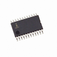
IC POT DGTL QUAD 10K OHM 24TSSOP
Manufacturer
Intersil
Series
XDCP™r
Datasheet
1.X9408WS24I.pdf
(20 pages)
Specifications of X9408WV24IZ-2.7T1
Taps
64
Resistance (ohms)
10K
Number Of Circuits
4
Temperature Coefficient
300 ppm/°C Typical
Memory Type
Non-Volatile
Interface
I²C, 2-Wire Serial
Voltage - Supply
2.7 V ~ 5.5 V
Operating Temperature
-40°C ~ 85°C
Mounting Type
Surface Mount
Package / Case
24-TSSOP
Resistance In Ohms
10K
Lead Free Status / RoHS Status
Lead free / RoHS Compliant
Other names
X9408WV24IZ-2.7T1TR


DC Electrical Specifications
NOTES:
ENDURANCE AND DATA RETENTION
CAPACITANCE
POWER-UP TIMING
NOTES:
Minimum endurance
Data retention
1. Absolute linearity is utilized to determine actual wiper voltage versus expected voltage as determined by wiper position when used as a
2. Relative linearity is utilized to determine the actual change in voltage between two successive tap positions when used as a potentiometer. It is
3. MI = RTOT/63 or [V(V
4. Limits should be considered typical and are not production tested.
5. t
6. Parameters with MIN and/or MAX limits are 100% tested at +25°C, unless otherwise specified. Temperature limits established by characterization
SYMBOL
t
C
t
C
R
t
PUW
PUR
I
I
I/O
potentiometer.
a measure of the error in step size.
SYMBOL
V
instruction can be issued
and are not production tested.
V
IN
CC1
CC2
I
I
V
PUR
V
SYMBOL
I
SB
LO
CC
LI
OL
IH
IL
(Note 4)
(Note 4)
(Note 5)
(Note 5)
(Note 6)
and t
V
V
read)
V
Input leakage current
Output leakage current
Input HIGH voltage
Input LOW voltage
Output LOW voltage
PUW
CC
CC
CC
PARAMETER
supply current (nonvolatile write)
supply current (move wiper, write,
current (standby)
Input/output capacitance (SDA)
Input capacitance (A0, A1, A2, A3, and SCL)
are the delays required from the time the third (last) power supply (V
Power-up to initiation of read operation
Power-up to initiation of write operation
V
CC
Power-up Ramp
H
PARAMETER
/R
H
) - V(V
12
L
/R
(Over recommended operating conditions unless otherwise stated.
L
)]/63, single pot
TEST
PARAMETER
f
Other Inputs = V
f
Other Inputs = V
SCL = SDA = V
I
SCL
SCL
OL
100,000
= 3mA
MIN
100
= 400kHz, SDA = Open,
= 400kHz, SDA = Open,
TEST CONDITIONS
X9408
CC
SS
SS
, Addr. = V
Data changes per bit per register
years
TEST CONDITION
SS
V
CC
V
I/O
IN
, V+ or V-) is stable until the specific
= 0V
= 0V
(Note 6)
MIN
0.2
V
(Note 6)
CC
–0.5
MIN
x 0.7
UNIT
(Note 4)
(Note 4)
(Note 6)
TYP
TYP
MAX
)
8
6
50
1
5
LIMITS
V
V
(Note 6)
CC
CC
MAX
250
0.4
10
10
5
3
x 0.1
+0.5
January 15, 2009
V/msec
UNIT
UNIT
pF
pF
ms
ms
FN8191.4
UNIT
mA
µA
µA
µA
µA
V
V
V
Related parts for X9408WV24IZ-2.7T1
Image
Part Number
Description
Manufacturer
Datasheet
Request
R

Part Number:
Description:
IC DCP QUAD 10K 64TP 24TSSOP
Manufacturer:
Intersil
Datasheet:
Part Number:
Description:
IC XDCP QUAD 64-TAP 10K 24-TSSOP
Manufacturer:
Intersil
Datasheet:
Part Number:
Description:
IC XDCP QUAD 64-TAP 10K 24-TSSOP
Manufacturer:
Intersil
Datasheet:
Part Number:
Description:
IC DCP QUAD 10K 64TP 24TSSOP
Manufacturer:
Intersil
Datasheet:
Part Number:
Description:
IC DCP QUAD 10K 64TP 24TSSOP
Manufacturer:
Intersil
Datasheet:
Part Number:
Description:
IC DCP QUAD 10K 64TP 24TSSOP
Manufacturer:
Intersil
Datasheet:
Part Number:
Description:
IC XDCP QUAD 64-TAP 10K 24-TSSOP
Manufacturer:
Intersil
Datasheet:

Part Number:
Description:
Intersil Corporation [CMOS Serial Controller Interface]
Manufacturer:
Intersil Corporation
Datasheet:
Part Number:
Description:
Manufacturer:
Intersil Corporation
Datasheet:
Part Number:
Description:
357-036-542-201 CARDEDGE 36POS DL .156 BLK LOPRO
Manufacturer:
Intersil Corporation
Datasheet:
Part Number:
Description:
1024-Word x 4-Bit LSI Static RAM
Manufacturer:
Intersil Corporation
Datasheet:
Part Number:
Description:
General Purpose NPN Transistor Arrays FN341.4
Manufacturer:
Intersil Corporation
Datasheet:
Part Number:
Description:
CMOS 16-Bit Microprocessor
Manufacturer:
Intersil Corporation
Datasheet:
Part Number:
Description:
Manufacturer:
Intersil Corporation
Datasheet:
Part Number:
Description:
Manufacturer:
Intersil Corporation
Datasheet: