ISL22317UFRTZ Intersil, ISL22317UFRTZ Datasheet - Page 11
ISL22317UFRTZ
Manufacturer Part Number
ISL22317UFRTZ
Description
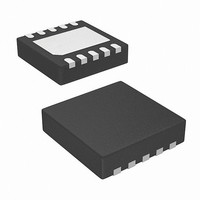
IC POT DGTL 128TP LN LP 10-TDFN
Manufacturer
Intersil
Series
XDCP™r
Datasheet
1.ISL22317TFRTZ-TK.pdf
(15 pages)
Specifications of ISL22317UFRTZ
Taps
128
Resistance (ohms)
50K
Number Of Circuits
1
Memory Type
Non-Volatile
Interface
I²C, 2-Wire Serial
Voltage - Supply
2.7 V ~ 5.5 V
Operating Temperature
-40°C ~ 125°C
Mounting Type
Surface Mount
Package / Case
10-TDFN Exposed Pad
Resistance In Ohms
50K
Lead Free Status / RoHS Status
Lead free / RoHS Compliant
Temperature Coefficient
-
Available stocks
Company
Part Number
Manufacturer
Quantity
Price
Company:

Part Number:
ISL22317UFRTZ-TK
Manufacturer:
Intersil
Quantity:
50


ISL22317. A maximum of two ISL22317 devices may occupy
the I
Principles of Operation
The ISL22317 is an integrated circuit incorporating one DCP
with its associated registers, non-volatile memory and an I
serial interface providing direct communication between a
host and the potentiometer and memory. The resistor array
is comprised of individual resistors connected in series. At
either end of the array and between each resistor, is an
electronic switch that transfers the potential at that point to
the wiper.
The electronic switches on the device operate in a “make
before break” mode when the wiper changes tap positions.
When the device is powered down, the last value stored in
IVR will be maintained in the non-volatile memory. When
power is restored, the contents of the IVR is recalled and
loaded into the WR to set the wiper to the initial value.
DCP Description
The DCP is implemented with a combination of resistor
elements and CMOS switches. The physical ends of each
DCP are equivalent to the fixed terminals of a mechanical
potentiometer (RH and RL pins). The RW pin of the DCP is
connected to intermediate nodes, and is equivalent to the
wiper terminal of a mechanical potentiometer. The position
of the wiper terminal within the DCP is controlled by a 7-bit
volatile Wiper Register (WR). When the WR of a DCP
contains all zeroes (WR<6:0>: 00h), its wiper terminal (RW)
is closest to its “Low” terminal (RL). When the WR register of
a DCP contains all ones (WR<6:0>: 7Fh), its wiper terminal
(RW) is closest to its “High” terminal (RH). As the value of
the WR increases from all zeroes (0) to all ones (127
decimal), the wiper moves monotonically from the position
closest to RL to the closest to RH.
While the ISL22317 is being powered up, the WR is reset to
40h (64 decimal), which locates RW roughly at the center
between RL and RH. After the power supply voltage
becomes large enough for reliable non-volatile memory
reading, the WR will be reload with the value stored in a
non-volatile Initial Value Register (IVR).
The WR and IVR can be read or written to directly using the
I
Memory Description
The ISL22317 contains one non-volatile 8-bit Initial Value
Register (IVR), one 8-bit non-volatile Mode Select Register
(MSR), and two volatile 8-bit registers: Wiper Register (WR)
and Access Control Register (ACR). Memory map of ISL22317
is in Table 1. The non-volatile register (IVR) at address 0,
contains initial wiper position and the volatile register (WR)
contains current wiper position.
2
C serial interface as described in the following sections.
2
C serial bus with addresses 50h and 54h.
11
2
C
ISL22317
The non-volatile IVR and volatile WR registers are
accessible with the same address 0.
The ISL22317 is pre-programed with 40h in the IVR.
The Access Control Register (ACR) at address 2 contains
information and control bits described below in Table 2.
The VOL bit (ACR<7>) determines whether the access is to
wiper registers WR or initial value registers IVR.
If VOL bit is 0, the non-volatile IVR register is accessible. If
VOL bit is 1, only the volatile WR is accessible. Note, value
is written to IVR register also is written to the WR. The
default value of this bit is 0.
The SHDN bit (ACR<6>) disables or enables Shutdown mode.
When this bit is 0, DCP is in Shutdown mode. Default value of
SHDN bit is 1.
The WIP bit (ACR<5>) is read only bit. It indicates that
non-volatile write operation is in progress. It is impossible to
write to the WR or ACR while WIP bit is 1.
The Mode Select Bit in Mode Select Register (MSR<7>) at
address 1 allows selection of Rheostat or Voltage Divider
Mode, see Table 3.
When this bit is 0, DCP is in two-terminal Rheostat Mode. In
Rheostat Mode, the RH pin should be left unconnected and
DCP can be used as variable resistor between RW and RL
pins.
When this bit is 1, DCP is in three-terminal Voltage Divider
Mode. In Voltage Divider Mode, signal is applied between
RH and RL terminals. Total resistance between RH and RL
terminals is precisely matched to external reference resistor.
Refer to reference resistor value in “Analog Specifications”
Table on page 3.
Default value of Mode Select Bit is 0.
The Precision Off bit (MSR<6>) allows the user to turn off
the matching mechanism and use the device as a regular,
Mode
Select
ADDRESS
(MSB)
(MSB)
VOL
(hex)
2
1
0
TABLE 2. ACCESS CONTROL REGISTER (ACR)
TABLE 3. MODE SELECT REGISTER (MSR)
Precision
Off
SHDN
Mode Select Register
NON-VOLATILE
TABLE 1. MEMORY MAP
WIP
IVR
NA
x
0
x
0
x
0
x
VOLATILE
ACR
WR
NA
0
x
April 15, 2010
FN6912.1
(LSB)
(LSB)
0
x
Related parts for ISL22317UFRTZ
Image
Part Number
Description
Manufacturer
Datasheet
Request
R

Part Number:
Description:
Precision Single Digitally Controlled Potentiometer
Manufacturer:
Intersil Corporation
Datasheet:
Part Number:
Description:
Intersil Corporation [CMOS Serial Controller Interface]
Manufacturer:
Intersil Corporation
Datasheet:
Part Number:
Description:
Manufacturer:
Intersil Corporation
Datasheet:
Part Number:
Description:
357-036-542-201 CARDEDGE 36POS DL .156 BLK LOPRO
Manufacturer:
Intersil Corporation
Datasheet:
Part Number:
Description:
1024-Word x 4-Bit LSI Static RAM
Manufacturer:
Intersil Corporation
Datasheet:
Part Number:
Description:
General Purpose NPN Transistor Arrays FN341.4
Manufacturer:
Intersil Corporation
Datasheet:
Part Number:
Description:
CMOS 16-Bit Microprocessor
Manufacturer:
Intersil Corporation
Datasheet:
Part Number:
Description:
Manufacturer:
Intersil Corporation
Datasheet:
Part Number:
Description:
Manufacturer:
Intersil Corporation
Datasheet:
Part Number:
Description:
Manufacturer:
Intersil Corporation
Datasheet:
Part Number:
Description:
Manufacturer:
Intersil Corporation
Datasheet:
Part Number:
Description:
CMOS 6-Bit Latch and Decoder Memory Interfaces
Manufacturer:
Intersil Corporation
Datasheet:
Part Number:
Description:
CA3046General Purpose NPN Transistor Arrays
Manufacturer:
Intersil Corporation
Datasheet:
Part Number:
Description:
Manufacturer:
Intersil Corporation
Datasheet:
Part Number:
Description:
TR909 DLC/FLC SLIC with Low Power Standby
Manufacturer:
Intersil Corporation
Datasheet: