ISL22326WFR16Z Intersil, ISL22326WFR16Z Datasheet - Page 11
ISL22326WFR16Z
Manufacturer Part Number
ISL22326WFR16Z
Description
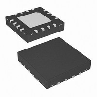
IC POT DGTL 128TP LN LP 16-QFN
Manufacturer
Intersil
Series
XDCP™r
Datasheet
1.ISL22326UFR16Z.pdf
(15 pages)
Specifications of ISL22326WFR16Z
Taps
128
Resistance (ohms)
10K
Number Of Circuits
2
Temperature Coefficient
50 ppm/°C Typical
Memory Type
Non-Volatile
Interface
I²C, 2-Wire Serial
Voltage - Supply
2.7 V ~ 5.5 V
Operating Temperature
-40°C ~ 125°C
Mounting Type
Surface Mount
Package / Case
16-VQFN Exposed Pad, 16-HVQFN, 16-SQFN, 16-DHVQFN
Resistance In Ohms
10K
Lead Free Status / RoHS Status
Lead free / RoHS Compliant
Available stocks
Company
Part Number
Manufacturer
Quantity
Price
Company:

Part Number:
ISL22326WFR16Z-TK
Manufacturer:
IXYS
Quantity:
12


The non-volatile IVRi and volatile WRi registers are accessible
with the same address.
The Access Control Register (ACR) contains information
and control bits described in Table 2. The VOL bit at access
control register (ACR[7]) determines whether the access is
to wiper registers WRi or initial value registers IVRi.
If VOL bit is 0, the non-volatile IVRi registers are accessible. If
VOL bit is 1, only the volatile WRi are accessible. Note, value
is written to IVRi register also is written to the corresponding
WRi. The default value of this bit is 0.
The SHDN bit (ACR[6]) disables or enables Shutdown mode.
This bit is logically ANDed with SHDN pin. When this bit is 0,
DCP is in Shutdown mode. Default value of SHDN bit is 1.
The WIP bit (ACR[5]) is read only bit. It indicates that
non-volatile write operation is in progress. It is impossible to
write to the IVRi, WRi or ACR while WIP bit is 1.
Shutdown Mode
The device can be put in Shutdown mode either by pulling the
SHDN pin to GND or setting the SHDN bit in the ACR register
to 0. The truth table for Shutdown mode is in Table 3.
I
The ISL22326 supports an I
protocol. The protocol defines any device that sends data
onto the bus as a transmitter and the receiving device as the
receiver. The device controlling the transfer is a master and
the device being controlled is the slave. The master always
initiates data transfers and provides the clock for both
2
ADDRESS
C Serial Interface
VOL
SHDN pin
8
7
6
5
4
3
2
1
0
High
High
TABLE 2. ACCESS CONTROL REGISTER (ACR)
Low
Low
SHDN
General Purpose
General Purpose
General Purpose
General Purpose
General Purpose
NON-VOLATILE
TABLE 1. MEMORY MAP
WIP
IVR1
IVR0
SHDN bit
—
1
1
0
0
TABLE 3.
2
11
C bidirectional bus oriented
0
Reserved
0
Normal operation
Not Available
Not Available
Not Available
Not Available
Not Available
0
Shutdown
Shutdown
Shutdown
VOLATILE
Mode
WR1
WR0
ACR
0
0
ISL22326
transmit and receive operations. Therefore, the ISL22326
operates as a slave device in all applications.
All communication over the I
sending the MSB of each byte of data first.
Protocol Conventions
Data states on the SDA line must change only during SCL
LOW periods. SDA state changes during SCL HIGH are
reserved for indicating START and STOP conditions
(see Figure 16). On power-up of the ISL22326, the SDA pin
is in the input mode.
All I
condition, which is a HIGH to LOW transition of SDA while
SCL is HIGH. The ISL22326 continuously monitors the SDA
and SCL lines for the START condition and does not
respond to any command until this condition is met (see
Figure 16). A START condition is ignored during the
power-up of the device.
All I
condition, which is a LOW to HIGH transition of SDA while
SCL is HIGH (see Figure 16). A STOP condition at the end
of a read operation, or at the end of a write operation places
the device in its standby mode.
An ACK, Acknowledge, is a software convention used to
indicate a successful data transfer. The transmitting device,
either master or slave, releases the SDA bus after
transmitting eight bits. During the ninth clock cycle, the
receiver pulls the SDA line LOW to acknowledge the
reception of the eight bits of data (see Figure 17).
The ISL22326 responds with an ACK after recognition of a
START condition followed by a valid Identification Byte, and
once again after successful receipt of an Address Byte. The
ISL22326 also responds with an ACK after receiving a Data
Byte of a write operation. The master must respond with an
ACK after receiving a Data Byte of a read operation.
A valid Identification Byte contains 1010 as the four MSBs,
and the following three bits matching the logic values present
at pins A2, A1, and A0. The LSB is the Read/Write bit. Its
value is “1” for a Read operation, and “0” for a Write operation
(see Table 4).
(MSB)
1
2
2
C interface operations must begin with a START
C interface operations must be terminated by a STOP
TABLE 4. IDENTIFICATION BYTE FORMAT
0
Logic values at pins A2, A1, and A0 respectively
1
0
2
C interface is conducted by
A2
A1
September 8, 2009
A0
FN6176.2
(LSB)
R/W
Related parts for ISL22326WFR16Z
Image
Part Number
Description
Manufacturer
Datasheet
Request
R

Part Number:
Description:
Manufacturer:
Intersil Corporation
Datasheet:
Part Number:
Description:
Intersil Corporation [CMOS Serial Controller Interface]
Manufacturer:
Intersil Corporation
Datasheet:
Part Number:
Description:
Manufacturer:
Intersil Corporation
Datasheet:
Part Number:
Description:
357-036-542-201 CARDEDGE 36POS DL .156 BLK LOPRO
Manufacturer:
Intersil Corporation
Datasheet:
Part Number:
Description:
1024-Word x 4-Bit LSI Static RAM
Manufacturer:
Intersil Corporation
Datasheet:
Part Number:
Description:
General Purpose NPN Transistor Arrays FN341.4
Manufacturer:
Intersil Corporation
Datasheet:
Part Number:
Description:
CMOS 16-Bit Microprocessor
Manufacturer:
Intersil Corporation
Datasheet:
Part Number:
Description:
Manufacturer:
Intersil Corporation
Datasheet:
Part Number:
Description:
Manufacturer:
Intersil Corporation
Datasheet:
Part Number:
Description:
Manufacturer:
Intersil Corporation
Datasheet:
Part Number:
Description:
Manufacturer:
Intersil Corporation
Datasheet:
Part Number:
Description:
CMOS 6-Bit Latch and Decoder Memory Interfaces
Manufacturer:
Intersil Corporation
Datasheet:
Part Number:
Description:
CA3046General Purpose NPN Transistor Arrays
Manufacturer:
Intersil Corporation
Datasheet:
Part Number:
Description:
Manufacturer:
Intersil Corporation
Datasheet:
Part Number:
Description:
TR909 DLC/FLC SLIC with Low Power Standby
Manufacturer:
Intersil Corporation
Datasheet: