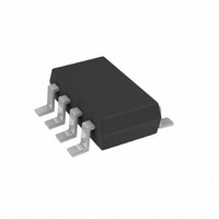
AD5228BUJZ100-R2 Analog Devices Inc, AD5228BUJZ100-R2 Datasheet - Page 4

AD5228BUJZ100-R2
Manufacturer Part Number
AD5228BUJZ100-R2
Description
IC DGTL POT 100K UP/DN TSOT23-8
Manufacturer
Analog Devices Inc
Specifications of AD5228BUJZ100-R2
Temperature Coefficient
35 ppm/°C Typical
Taps
32
Resistance (ohms)
100K
Number Of Circuits
1
Memory Type
Volatile
Interface
Up/Down Counter
Voltage - Supply
2.7 V ~ 5.5 V
Operating Temperature
-40°C ~ 105°C
Mounting Type
Surface Mount
Package / Case
TSOT-23-8, TSOT-8
Resistance In Ohms
100K
End To End Resistance
100kohm
No. Of Steps
32
Resistance Tolerance
± 20%
Supply Voltage Range
2.7V To 5.5V
Control Interface
Pushbutton
No. Of Pots
Single
Lead Free Status / RoHS Status
Lead free / RoHS Compliant
For Use With
EVAL-AD5228EBZ - BOARD EVAL FOR AD5228 DGTL POT
Lead Free Status / RoHS Status
Lead free / RoHS Compliant, Lead free / RoHS Compliant
Available stocks
Company
Part Number
Manufacturer
Quantity
Price
Company:
Part Number:
AD5228BUJZ100-R2
Manufacturer:
AD
Quantity:
15 562
AD5228
Parameter
DYNAMIC CHARACTERISTICS
1
2
3
4
5
6
7
8
9
10
11
12
INTERFACE TIMING DIAGRAMS
Typicals represent average readings at 25°C, V
Resistor position nonlinearity error, R-INL, is the deviation from an ideal value measured between the maximum resistance and the minimum resistance wiper
positions. R-DNL measures the relative step change from ideal between successive tap positions. Parts are guaranteed monotonic.
INL and DNL are measured at V
Guaranteed by design and not subject to production test.
DNL specification limits of ±1 LSB maximum are guaranteed monotonic operating conditions.
Resistor Terminals A, B, and W have no limitations on polarity with respect to each other.
PU and PD have 100 kΩ internal pull-up resistors, I
P
dissipation.
Bandwidth, noise, and settling time are dependent on the terminal resistance value chosen. The lowest R value results in the fastest settling time and highest
bandwidth. The highest R value results in the minimum overall power consumption.
using V
bounce is met and allows the AD5228 to increment by one step. If the PU signal remains at low and reaches t
characteristics apply to PD operation.
All dynamic characteristics use V
Note that all input control voltages are specified with t
The debouncer keeps monitoring the logic-low level once PU is connected to ground. Once the signal lasts longer than 11 ms, the debouncer assumes the last
DISS
Built-in Debounce and Settling Time
PU Low Pulse Width
PD Low Pulse Width
PU High Repetitive Pulse Width
PD High Repetitive Pulse Width
Autoscan Start Time
Autoscan Time
Bandwidth –3 dB
Total Harmonic Distortion
Resistor Noise Voltage
R
R
PU
WB
PU
WB
is calculated based on I
DD
= 5 V.
t
Figure 3. Increment R
AS_START
Figure 2. Increment R
t
DB
t
DB
t
PU
DD_STBY
W
t
AS
with the RDAC configured as a potentiometer divider similar to a voltage output D/A converter. V
DD
4, 9, 10, 11
× V
t
PU_REP
= 5 V.
DD
WB
WB
only. I
in Autoscan Mode
in Discrete Steps
DD_ACT
12
DD
= 5 V.
DD_ACT
duration should be short. Users should not hold PU or PD pin to ground longer than necessary to elevate power
R
= V
= t
DD
F
= 1 ns (10% to 90% of V
/100 kΩ + I
Symbol
t
t
t
t
t
t
t
BW_10
BW_50
BW_100
THD
e
DB
PU
PD
PU_REP
PD_REP
AS_START
AS
N_WB
OSC
Rev. A | Page 4 of 20
(internal oscillator operating current) when PU or PD is connected to ground.
DD
) and timed from a voltage level of 1.6 V. Switching characteristics are measured
Conditions
PU or PD = 0 V
PU or PD = 0 V
R
R
R
V
V
R
AB
AB
AB
A
B
WB
= 0 V dc, f = 1 kHz
= 1 V rms, R
R
R
= 10 kΩ, midscale
= 50 kΩ, midscale
= 100 kΩ, midscale
= 5 kΩ, f = 1 kHz
PD
WB
PU
WB
AB
t
AS_START
Figure 5. Decrement R
Figure 4. Decrement R
= 10 kΩ,
AS_START
t
DB
, the AD5528 increments again, see Figure 7. Similar
t
PD
t
AS
t
DB
t
PD_REP
Min
6
12
12
1
1
0.6
0.16
WB
WB
A
in Autoscan Mode
= V
in Discrete Steps
DD
Typ
0.8
0.25
460
100
50
0.05
14
and V
1
B
= 0 V.
Max
1.2
0.38
Unit
ms
ms
ms
μs
μs
s
s
kHz
kHz
kHz
%
nV/√Hz


