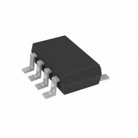
AD5228BUJZ100-R2 Analog Devices Inc, AD5228BUJZ100-R2 Datasheet - Page 15

AD5228BUJZ100-R2
Manufacturer Part Number
AD5228BUJZ100-R2
Description
IC DGTL POT 100K UP/DN TSOT23-8
Manufacturer
Analog Devices Inc
Specifications of AD5228BUJZ100-R2
Temperature Coefficient
35 ppm/°C Typical
Taps
32
Resistance (ohms)
100K
Number Of Circuits
1
Memory Type
Volatile
Interface
Up/Down Counter
Voltage - Supply
2.7 V ~ 5.5 V
Operating Temperature
-40°C ~ 105°C
Mounting Type
Surface Mount
Package / Case
TSOT-23-8, TSOT-8
Resistance In Ohms
100K
End To End Resistance
100kohm
No. Of Steps
32
Resistance Tolerance
± 20%
Supply Voltage Range
2.7V To 5.5V
Control Interface
Pushbutton
No. Of Pots
Single
Lead Free Status / RoHS Status
Lead free / RoHS Compliant
For Use With
EVAL-AD5228EBZ - BOARD EVAL FOR AD5228 DGTL POT
Lead Free Status / RoHS Status
Lead free / RoHS Compliant, Lead free / RoHS Compliant
Available stocks
Company
Part Number
Manufacturer
Quantity
Price
Company:
Part Number:
AD5228BUJZ100-R2
Manufacturer:
AD
Quantity:
15 562
APPLICATIONS
MANUAL ADJUSTABLE LED DRIVER
The AD5228 can be used in many electronics-level adjustments
such as LED drivers for LCD panel backlight controls. Figure 41
shows a manually adjustable LED driver. The AD5228 sets the
voltage across the white LED D1 for the brightness control.
Since U2 handles up to 250 mA, a typical white LED with V
3.5 V requires a resistor, R1, to limit U2 current. This circuit is
simple but not power efficient. The U2 shutdown pin can be
toggled with a PWM signal to conserve power.
ADJUSTABLE CURRENT SOURCE FOR LED DRIVER
Because LED brightness is a function of current rather than of
forward voltage, an adjustable current source is preferred as
shown in Figure 42. The load current can be found as the V
of the AD5228 divided by R
The U1 ADP3333ARM-1.5 is a 1.5 V LDO that is lifted above
or lowered below 0 V. When V
minimum, there is no current through D1, so the GND pin of U1
is at –1.5 V if U3 is biased with the dual supplies. As a result,
some of the U2 low resistance steps have no effect on the output
until the U1 GND pin is lifted above 0 V. When V
AD5228 is at its maximum, V
supply voltage must be biased with adequate headroom. Similarly,
PWM signal can be applied at the U1 shutdown pin for power
efficiency.
5V
I
PWM
D1
C1
1μF
PUSH-DOWN
=
PUSH-UP
BUTTON
BUTTON
V
SD
R
ADP3333
IN
V
ARM-1.5
WB
SET
C2
0.1μF
U1
GND
Figure 41. Low Cost Adjustable LED Driver
V
OUT
PU
PD
PUSH-DOWN
V
PUSH-UP
BUTTON
BUTTON
5V
DD
PRE
5V
AD5228
A
10kΩ
B
GND
SET
U1
W
OUT
V
PRE
PU
PD
.
DD
WB
GND
becomes VL + V
of the AD5228 is at its
AD5228
B
10kΩ
A
R1
418kΩ
V+
AD8591
V–
–
+
AD8591
5V
5V
U3
U2
W
U2
V+
V–
PWM
0.1μF
–
+
C3
SD
6Ω
R1
AB
R
0.1Ω
WB
D1
SET
, so the U1
VL
of the
WHITE
LED
D1
ID
WB
F
Rev. A | Page 15 of 20
of
(7)
ADJUSTABLE HIGH POWER LED DRIVER
The previous circuit works well for a single LED. Figure 43
shows a circuit that can drive three to four high power LEDs.
The ADP1610 is an adjustable boost regulator that provides the
voltage headroom and current for the LEDs. The AD5228 and
the op amp form an average gain of 12 feedback network that
servos the R
reference voltage. As the loop is set, the voltage across R
regulated around 0.1 V and adjusted by the digital
potentiometer.
R
to limit maximum LED current. R3 should also be used in par-
allel with AD5228 to limit the LED current within an achievable
range. A wider current adjustment range is possible by lowering
the R2 to R1 ratio as well as changing R3 accordingly.
5V
SET
L1–SLF6025-100M1R0
D1–MBR0520LT1
10μF
should be small enough to conserve power but large enough
C2
I
LED
Figure 43. Adjustable Current Source for LEDs in Series
=
Figure 42. Adjustable Current Source for LED Driver
13.5kΩ
V
SET
R
R
SET
SET
R4
voltage and the ADP1610 FB pin 1.2 V band gap
390pF
PWM
1.2V
100kΩ
C
R
C
C
1.1kΩ
0.1μF
R2
U1
C8
AD8541
SD
FB
COMP
SS
V+
V–
ADP1610
10nF
C
5V
SS
U3
U2
RT GND
+
–
IN
SW
B
W
10kΩ
200Ω
R3
AD5228
L1
10μF
U1
D1
A
100Ω
R1
0.25Ω
C3
10μF
R
SET
AD5228
SET
D2
D3
D4
is
V
OUT
(8)


