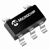
MCP4014T-202E/OT Microchip Technology, MCP4014T-202E/OT Datasheet - Page 27

MCP4014T-202E/OT
Manufacturer Part Number
MCP4014T-202E/OT
Description
IC DGTL POT 2.1K 1CH RHE SOT23-5
Manufacturer
Microchip Technology
Specifications of MCP4014T-202E/OT
Taps
64
Resistance (ohms)
2.1K
Number Of Circuits
1
Temperature Coefficient
150 ppm/°C Typical
Memory Type
Volatile
Interface
Up/Down
Voltage - Supply
1.8 V ~ 5.5 V
Operating Temperature
-40°C ~ 125°C
Mounting Type
Surface Mount
Package / Case
SOT-23-5, SC-74A, SOT-25
Resistance In Ohms
2.10K
End To End Resistance
2.1kohm
No. Of Steps
64
Resistance Tolerance
± 20%
Supply Voltage Range
2.7V To 5.5V
Control Interface
2 Wire, Serial
No. Of Pots
Single
Lead Free Status / RoHS Status
Lead free / RoHS Compliant
Other names
MCP4014T-202E/OTTR
4.2
When the device powers up (rising V
Trip Point Voltage (V
restored. Table 4-1 shows the default value loaded into
the wiper on POR/BOR.
TABLE 4-1:
While V
may not meet the data sheet specifications (see
Figure 4-2). The wiper state may be unknown. Also, the
device may be capable of incrementing or decrement-
ing, if a valid command is detected on the CS and U/D
pins.
FIGURE 4-2:
© 2005 Microchip Technology Inc.
-202
-502
-103
-503
Package
Code
DD
Power-up
V
1.8V
V
V
< V
DD
TP
SS
Mid-scale
Mid-scale
Mid-scale
Mid-scale
Default
Setting
min
Wiper
POR
DEFAULT POR WIPER
SETTING SELECTION
(1.8V), the electrical performance
TP
Power-up and Brown-out.
)), the “default” wiper setting is
Wiper
Code
1Fh
1Fh
1Fh
1Fh
DD
R
crosses the
10.0 k
50.0 k
Typical
AB
2.1 k
5.0 k
POR Trip Point (on Rising V
Value
Outside Device Operation
4.3
If the device V
age, care must be taken to ensure that the CS and U/D
pins do not “create” any of the serial commands.
When the device V
electrical performance may not meet the data sheet
specifications (see Figure 4-2). The wiper state may be
unknown. Also, the device may be capable of incre-
menting or decrementing, if a valid command is
detected on the CS and U/D pins.
When the device voltage rises from below the power-
up trip point (V
range, the wiper state will be forced to the default POR
wiper setting (see Table 4-1).
4.4
The serial interface is inactive any time the CS pin is at
V
IH
and all write cycles are completed.
DD
)
Brown Out
Serial Interface Inactive
Wiper Forced to Default POR Setting
DD
MCP4011/2/3/4
TP
is below the specified minimum volt-
) into the valid operation voltage
DD
drops below V
DS21978A-page 27
MIN
(1.8V), the


