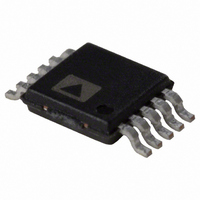
AD5258BRMZ10 Analog Devices Inc, AD5258BRMZ10 Datasheet - Page 19

AD5258BRMZ10
Manufacturer Part Number
AD5258BRMZ10
Description
IC POT DGTL I2C 10K 64P 10MSOP
Manufacturer
Analog Devices Inc
Datasheet
1.AD5258BRMZ100.pdf
(24 pages)
Specifications of AD5258BRMZ10
Memory Type
Non-Volatile
Taps
64
Resistance (ohms)
10K
Number Of Circuits
1
Temperature Coefficient
200 ppm/°C Typical
Interface
I²C, 2-Wire Serial
Voltage - Supply
2.7 V ~ 5.5 V
Operating Temperature
-40°C ~ 85°C
Mounting Type
Surface Mount
Package / Case
10-MSOP, Micro10™, 10-uMAX, 10-uSOP
Resistance In Ohms
10K
End To End Resistance
10kohm
Resistance Tolerance
± 30%
No. Of Steps
64
Supply Voltage Range
2.7V To 5.5V
Control Interface
I2C, Serial
No. Of Pots
Single
Lead Free Status / RoHS Status
Lead free / RoHS Compliant
For Use With
AD5258EVAL - BOARD EVAL FOR AD5258 DGTL POT
Lead Free Status / RoHS Status
Lead free / RoHS Compliant, Lead free / RoHS Compliant
Available stocks
Company
Part Number
Manufacturer
Quantity
Price
Company:
Part Number:
AD5258BRMZ10
Manufacturer:
ADI
Quantity:
835
Company:
Part Number:
AD5258BRMZ10
Manufacturer:
AD
Quantity:
2 444
Part Number:
AD5258BRMZ10
Manufacturer:
ADI/亚德诺
Quantity:
20 000
Part Number:
AD5258BRMZ10-R7
Manufacturer:
ADI/亚德诺
Quantity:
20 000
Part Number:
AD5258BRMZ100
Manufacturer:
ADI/亚德诺
Quantity:
20 000
ESD PROTECTION OF DIGITAL PINS AND
RESISTOR TERMINALS
The AD5258 V
boundary conditions for proper 3-terminal and digital input
operation. Supply signals present on Terminal A, Terminal B,
and Terminal W that exceed V
internal forward-biased ESD protection diodes (see Figure 40).
Digital Input SCL and Digital Input SDA are clamped by ESD
protection diodes with respect to V
Figure 41.
POWER-UP SEQUENCE
Because the ESD protection diodes limit the voltage compliance
at Terminal A, Terminal B, and Terminal W (see Figure 40), it is
important to power GND/V
age to Terminal A, Terminal B, and Terminal W; otherwise, the
diode is forward-biased such that V
unintentionally and may affect the user’s circuit. The ideal
power-up sequence is in the following order: GND, V
V
of powering V
as long as they are powered after GND, V
LAYOUT AND POWER SUPPLY BYPASSING
It is good practice to employ compact, minimum lead length
layout design. The leads to the inputs should be as direct as
possible with minimum conductor length. Ground paths
should have low resistance and low inductance.
LOGIC
, digital inputs, and then V
Figure 41. Maximum Terminal Voltages Set by V
Figure 40. Maximum Terminal Voltages Set by V
A
DD
, V
, V
B
, V
LOGIC
W
and the digital inputs is not important
, and GND power supplies define the
DD
/V
DD
A
LOGIC
or GND are clamped by the
, V
LOGIC
DD
B
, V
before applying any volt-
and V
and GND as shown in
W
V
A
W
B
GND
V
SCL
GND
SDA
DD
DD
. The relative order
LOGIC
, and V
LOGIC
LOGIC
DD
and GND
are powered
and GND
LOGIC
DD
.
,
Rev. C | Page 19 of 24
Similarly, it is also good practice to bypass the power supplies
with quality capacitors for optimum stability. Supply leads to
the device should be bypassed with disc or chip ceramic capaci-
tors of 0.01 μF to 0.1 μF. In addition, low ESR 1 μF to 10 μF
tantalum or electrolytic capacitors should be applied at the
supplies to minimize any transient disturbance and low fre-
quency ripple (see Figure 42). As well, the digital ground
should be joined remotely to the analog ground at one point
to minimize the ground bounce.
MULTIPLE DEVICES ON ONE BUS
The AD5258 has two configurable address pins, AD0 and AD1.
The state of these two pins is registered upon power-up and
decoded into a corresponding I
Table 5). This allows up to four devices on the bus to be written
to or read from independently.
EVALUATION BOARD
An evaluation board, along with all necessary software, is
available to program the AD5258 from any PC running
Windows® 98/Windows 2000/Windows XP. The graphical
user interface, as shown in Figure 43, is straightforward and
easy to use. More detailed information is available in the user
manual that comes with the board.
V
Figure 43. AD5258 Evaluation Board Software
DD
10µF
Figure 42. Power Supply Bypassing
C2
+
0.1µF
C1
2
C-compatible 7-bit address (see
V
DD
AD5258
GND
AD5258


