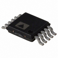
AD5258BRMZ10 Analog Devices Inc, AD5258BRMZ10 Datasheet - Page 15

AD5258BRMZ10
Manufacturer Part Number
AD5258BRMZ10
Description
IC POT DGTL I2C 10K 64P 10MSOP
Manufacturer
Analog Devices Inc
Datasheet
1.AD5258BRMZ100.pdf
(24 pages)
Specifications of AD5258BRMZ10
Memory Type
Non-Volatile
Taps
64
Resistance (ohms)
10K
Number Of Circuits
1
Temperature Coefficient
200 ppm/°C Typical
Interface
I²C, 2-Wire Serial
Voltage - Supply
2.7 V ~ 5.5 V
Operating Temperature
-40°C ~ 85°C
Mounting Type
Surface Mount
Package / Case
10-MSOP, Micro10™, 10-uMAX, 10-uSOP
Resistance In Ohms
10K
End To End Resistance
10kohm
Resistance Tolerance
± 30%
No. Of Steps
64
Supply Voltage Range
2.7V To 5.5V
Control Interface
I2C, Serial
No. Of Pots
Single
Lead Free Status / RoHS Status
Lead free / RoHS Compliant
For Use With
AD5258EVAL - BOARD EVAL FOR AD5258 DGTL POT
Lead Free Status / RoHS Status
Lead free / RoHS Compliant, Lead free / RoHS Compliant
Available stocks
Company
Part Number
Manufacturer
Quantity
Price
Company:
Part Number:
AD5258BRMZ10
Manufacturer:
ADI
Quantity:
835
Company:
Part Number:
AD5258BRMZ10
Manufacturer:
AD
Quantity:
2 444
Part Number:
AD5258BRMZ10
Manufacturer:
ADI/亚德诺
Quantity:
20 000
Part Number:
AD5258BRMZ10-R7
Manufacturer:
ADI/亚德诺
Quantity:
20 000
Part Number:
AD5258BRMZ100
Manufacturer:
ADI/亚德诺
Quantity:
20 000
I
Note that the wiper’s default value prior to programming the
EEPROM is midscale.
The master initiates a data transfer by establishing a start con-
dition when a high-to-low transition on the SDA line occurs
while SCL is high (see Figure 3). The next byte is the slave
address byte, which consists of the slave address (first seven bits)
followed by an R/ W bit (see Table 6). When the R/ W bit is high,
the master reads from the slave device. When the R/ W bit is
low, the master writes to the slave device.
The slave address of the part is determined by two configurable
address pins, AD0 and AD1. The state of these two pins is regis-
tered upon power-up and decoded into a corresponding I
7-bit address (see Table 5). The slave address corresponding to
the transmitted address bits responds by pulling the SDA line
low during the ninth clock pulse (this is termed the slave
acknowledge bit).
At this stage, all other devices on the bus remain idle while the
selected device waits for data to be written to or read from its
serial register.
WRITING
In the write mode, the last bit (R/ W ) of the slave address byte is
logic low. The second byte is the instruction byte. The first three
bits of the instruction byte are the command bits (see Table 6).
The user must choose whether to write to the RDAC register or
EEPROM register or to activate the software write protect (see
Table 7 to Table 10). The final five bits are all zeros (see Table 13
and Table 14). The slave again responds by pulling the SDA line
low during the ninth clock pulse.
The final byte is the data byte MSB first. Don’t cares can be
left either high or low. In the case of the write protect mode,
data is not stored; rather, a logic high in the LSB enables write
protect. Likewise, a logic low disables write protect. The slave
again responds by pulling the SDA line low during the ninth
clock pulse.
STORING/RESTORING
In this mode, only the address and instruction bytes are nec-
essary. The last bit (R/ W ) of the address byte is logic low. The
first three bits of the instruction byte are the command bits
(see Table 6). The two choices are transfer data from RDAC-
to-EEPROM (store) or from EEPROM-to-RDAC (restore).
The final five bits are all zeros (see Table 13 and Table 14). In
addition, users should issue an NOP command immediately
after restoring the EEMEM setting to RDAC, thereby mini-
mizing supply current dissipation.
2
C INTERFACE
2
C
Rev. C | Page 15 of 24
READING
Assuming the register of interest was not just written to, it is
necessary to write a dummy address and instruction byte. The
instruction byte will vary depending on whether the data that
is wanted is the RDAC register, EEPROM register, or tolerance
register (see Table 11 to Table 16).
After the dummy address and instruction bytes are sent, a repeat
start is necessary. After the repeat start, another address byte is
needed, except this time the R/ W bit is logic high. Following
this address byte is the readback byte containing the informa-
tion requested in the instruction byte. Read bits appear on the
negative edges of the clock. Don’t cares may be in either a high
or low state.
The tolerance register can be read back individually (see
Table 15) or consecutively (see Table 16). Refer to the Read
Modes section for detailed information on the interpretation
of the tolerance bytes.
After all data bits have been read or written, a stop condition is
established by the master. A stop condition is defined as a low-
to-high transition on the SDA line while SCL is high. In write
mode, the master pulls the SDA line high during the 10
pulse to establish a stop condition (see Table 8). In read mode,
the master issues a no acknowledge for the ninth clock pulse
(that is, the SDA line remains high). The master then brings the
SDA line low before the 10
establish a stop condition (see Table 11).
A repeated write function provides the user with the flexibility
of updating the RDAC output multiple times after addressing
and instructing the part only once. For example, after the RDAC
has acknowledged its slave address and instruction bytes in the
write mode, the RDAC output is updated on each successive
byte until a stop condition is received. If different instructions
are needed, the write/read mode must restart with a new slave
address, instruction, and data byte. Similarly, a repeated read
function of the RDAC is also allowed.
th
clock pulse and raises SDA high to
AD5258
th
clock


