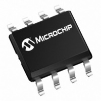
MCP4561-104E/MS Microchip Technology, MCP4561-104E/MS Datasheet - Page 50

MCP4561-104E/MS
Manufacturer Part Number
MCP4561-104E/MS
Description
IC DGTL POT 100K 256TAPS 8-MSOP
Manufacturer
Microchip Technology
Datasheet
1.MCP4541T-502EMF.pdf
(92 pages)
Specifications of MCP4561-104E/MS
Package / Case
8-MSOP, Micro8™, 8-uMAX, 8-uSOP,
Taps
257
Resistance (ohms)
100K
Number Of Circuits
1
Temperature Coefficient
150 ppm/°C Typical
Memory Type
Non-Volatile
Interface
I²C, 2-Wire Serial
Voltage - Supply
2.7 V ~ 5.5 V
Operating Temperature
-40°C ~ 125°C
Mounting Type
Surface Mount
Resistance In Ohms
100K
Number Of Pots
Single
Taps Per Pot
256
Resistance
100 KOhms
Wiper Memory
Non Volatile
Digital Interface
Serial (2-Wire, I2C)
Operating Supply Voltage
2.5 V, 3.3 V, 5 V
Supply Current
2.5 uA
Maximum Operating Temperature
+ 125 C
Minimum Operating Temperature
- 40 C
Mounting Style
SMD/SMT
Supply Voltage (max)
5.5 V
Supply Voltage (min)
1.8 V
Lead Free Status / RoHS Status
Lead free / RoHS Compliant
Lead Free Status / RoHS Status
Lead free / RoHS Compliant, Lead free / RoHS Compliant
Available stocks
Company
Part Number
Manufacturer
Quantity
Price
Company:
Part Number:
MCP4561-104E/MS
Manufacturer:
MICROCHIP
Quantity:
12 000
MCP454X/456X/464X/466X
6.2.4
The address byte is the first byte received following the
START condition from the master device. The address
contains four (or more) fixed bits and (up to) three user
defined hardware address bits (pins A2, A1, and A0).
These 7-bits address the desired I
A7:A4 address bits are fixed to “0101” and the device
appends the value of following three address pins (A2,
A1, A0). Address pins that are not present on the
device are pulled up (a bit value of ‘1’).
Since there are up to three adress bits controlled by
hardware pins, there may be up to eight MCP4XXX
devices on the same I
Figure 6-9
contains the seven address bits. There is also a read/
write bit.
Hardware Address Pins
The hardware address bits (A2, A1, and A0)
correspond to the logic level on the associated address
pins. This allows up to eight devices on the bus.
These pins have a weak pull-up enabled when the V
< V
technology and exhibits the same characteristics as the
High-voltage tolerant I/O structure.
The state of the A0 address pin is latch on POR/BOR.
This is required since High Voltage commands force
this pin (HVC/A0) to the V
DS22107A-page 50
BOR
. The weak pull-up utilizes the “smart” pull-up
Table 6-2
shows the slave address byte format, which
ADDRESSING
shows the fixed address for device.
2
C bus.
IHH
level.
2
C device. The
DD
FIGURE 6-9:
I
TABLE 6-2:
6.2.5
The MCP45XX/46XX implements slope control on the
SDA output.
As the device transitions from HS mode to FS mode,
the slope control parmameter will change from the HS
specification to the FS specification.
For Fast (FS) and High-Speed (HS) modes, the device
has a spike suppression and a Schmidt trigger at SDA
and SCL inputs.
2
Start
bit
Device
MCP45X1 ‘0101 11’b + A0
MCP45X2 ‘0101 1’b + A1:A0
MCP46X1 ‘0101’b + A2:A1:A0 Supports up to 8
MCP46X2 ‘0101 1’b + A1:A0
Note 1:
A = 0 = Slave Device Acknowledges byte
A = 1 = Slave Device does not Acknowledge byte
A bit (controlled by slave device)
S A6 A5 A4 A3 A2 A1 A0 R/W A/A
C Control Byte.
“0” “1” “0” “1”
A0 is used for High-Voltage commands
and the value is latched at POR.
SLOPE CONTROL
Address
Slave Address
DEVICE SLAVE ADDRESSES
Slave Address Bits in the
See
© 2008 Microchip Technology Inc.
R/W = 0 = write
R/W = 1 = read
R/W bit
Table 6-2
Comment
Supports up to 2
devices. Note 1
Supports up to 4
devices. Note 1
devices. Note 1
Supports up to 4
devices. Note 1


