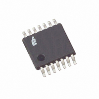
X95820WV14IZ-2.7T1 Intersil, X95820WV14IZ-2.7T1 Datasheet - Page 11

X95820WV14IZ-2.7T1
Manufacturer Part Number
X95820WV14IZ-2.7T1
Description
IC POT DGTL DUAL 10K OHM 14TSSOP
Manufacturer
Intersil
Series
XDCP™r
Datasheet
1.X95820WV14IZ-2.7T1.pdf
(12 pages)
Specifications of X95820WV14IZ-2.7T1
Taps
256
Resistance (ohms)
10K
Number Of Circuits
2
Temperature Coefficient
45 ppm/°C Typical
Memory Type
Non-Volatile
Interface
I²C, 2-Wire Serial
Voltage - Supply
2.7 V ~ 5.5 V
Operating Temperature
-40°C ~ 85°C
Mounting Type
Surface Mount
Package / Case
14-TSSOP
Resistance In Ohms
10K
Number Of Elements
2
# Of Taps
256
Resistance (max)
10KOhm
Power Supply Requirement
Single
Interface Type
Serial (I2C)
Single Supply Voltage (typ)
3.3V
Dual Supply Voltage (typ)
Not RequiredV
Single Supply Voltage (min)
2.7V
Single Supply Voltage (max)
5.5V
Dual Supply Voltage (min)
Not RequiredV
Dual Supply Voltage (max)
Not RequiredV
Operating Temp Range
-40C to 85C
Operating Temperature Classification
Industrial
Mounting
Surface Mount
Pin Count
14
Package Type
TSSOP
Lead Free Status / RoHS Status
Lead free / RoHS Compliant
Other names
X95820WV14IZ-2.7T1TR
Available stocks
Company
Part Number
Manufacturer
Quantity
Price
Part Number:
X95820WV14IZ-2.7T1
Manufacturer:
INTERSIL
Quantity:
20 000
Write Operation
A Write operation requires a START condition, followed by a
valid Identification Byte, a valid Address Byte, a Data Byte,
and a STOP condition. After each of the three bytes, the
X95820 responds with an ACK. At this time, if the Data Byte
is to be written only to volatile registers, then the device
enters its standby state. If the Data Byte is to be written also
to non-volatile memory, the X95820 begins its internal write
cycle to non-volatile memory. During the internal non-volatile
write cycle, the device ignores transitions at the SDA and
SCL pins, and the SDA output is at a high impedance state.
When the internal non-volatile write cycle is completed, the
X95820 enters its standby state (See Figure 17).
The byte at address 00001000 bin (8 decimal) determines if
the Data Byte is to be written to volatile and/or non-volatile
memory. See “Memory Description” on page 9.
Data Protection
The WP pin has to be at logic HIGH to perform any Write
operation to the device. When the WP is active (LOW) the
device ignores Data Bytes of a Write Operation, does not
respond to the Data Bytes with an ACK, and instead, goes to
its standby state waiting for a new START condition.
A STOP condition also acts as a protection of non-volatile
memory. A valid Identification Byte, Address Byte, and total
number of SCL pulses act as a protection of both volatile
and non-volatile registers. During a Write sequence, the
Data Byte is loaded into an internal shift register as it is
received. If the Address Byte is 0, 1, or 8 decimal, the Data
Byte is transferred to the appropriate Wiper Register (WR) or
to the Access Control Register, at the falling edge of the SCL
Signal at SDA
Signals from the
from the
Signals
Master
Slave
S
a
t
r
t
1
0
Identification
1
R/W=0
0
Byte
with
11
0
A
C
K
Address
Byte
FIGURE 18. READ SEQUENCE
A
C
K
S
a
r
t
t
X95820
1
Identification
0
1
R/W=1
Byte
with
0
pulse that loads the last bit (LSB) of the Data Byte. If the
Address Byte is between 0 and 6 (inclusive), and the Access
Control Register is all zeros (default), then the STOP
condition initiates the internal write cycle to non-volatile
memory.
Read Operation
A Read operation consists of a three byte instruction
followed by one or more Data Bytes (See Figure 18). The
master initiates the operation issuing the following
sequence: a START, the Identification byte with the R/W bit
set to “0”, an Address Byte, a second START, and a second
Identification byte with the R/W bit set to “1”. After each of
the three bytes, the X95820 responds with an ACK. Then the
X95820 transmits Data Bytes as long as the master
responds with an ACK during the SCL cycle following the
eight bit of each byte. The master terminates the read
operation (issuing a STOP condition) following the last bit of
the last Data Byte (See Figure 18).
The Data Bytes are from the memory location indicated by
an internal pointer. This pointer initial value is determined by
the Address Byte in the Read operation instruction, and
increments by one during transmission of each Data Byte.
After reaching the memory location 01Fh (8 decimal) the
pointer “rolls over” to 00h, and the device continues to output
data for each ACK received.
The byte at address 00001000 bin (8 decimal) determines if
the Data Bytes being read are from volatile or non-volatile
memory. See “Memory Description” on page 9.
1
A
C
K
First Read Data
Byte
A
C
K
A
C
K
Last Read Data
Byte
July 18, 2006
FN8212.2
S
o
p
t


