X95820WV14IZ-2.7T1 Intersil, X95820WV14IZ-2.7T1 Datasheet
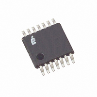
IC POT DGTL DUAL 10K OHM 14TSSOP

X95820WV14IZ-2.7T1

Manufacturer Part Number
X95820WV14IZ-2.7T1
Description
IC POT DGTL DUAL 10K OHM 14TSSOP
Manufacturer
Intersil
Series
XDCP™r
Datasheet

Specifications of X95820WV14IZ-2.7T1

Taps
256
Resistance (ohms)
10K
Number Of Circuits
2
Temperature Coefficient
45 ppm/°C Typical
Memory Type
Non-Volatile
Interface
I²C, 2-Wire Serial
Voltage - Supply
2.7 V ~ 5.5 V
Operating Temperature
-40°C ~ 85°C
Mounting Type
Surface Mount
Package / Case
14-TSSOP
Resistance In Ohms
10K
Number Of Elements
2
# Of Taps
256
Resistance (max)
10KOhm
Power Supply Requirement
Single
Interface Type
Serial (I2C)
Single Supply Voltage (typ)
3.3V
Dual Supply Voltage (typ)
Not RequiredV
Single Supply Voltage (min)
2.7V
Single Supply Voltage (max)
5.5V
Dual Supply Voltage (min)
Not RequiredV
Dual Supply Voltage (max)
Not RequiredV
Operating Temp Range
-40C to 85C
Operating Temperature Classification
Industrial
Mounting
Surface Mount
Pin Count
14
Package Type
TSSOP
Lead Free Status / RoHS Status
Lead free / RoHS Compliant
Other names
X95820WV14IZ-2.7T1TR

Available stocks

Company
Part Number
Manufacturer
Quantity
Price
Part Number:
X95820WV14IZ-2.7T1
Manufacturer:
INTERSIL
Quantity:
20 000
Low Noise/Low Power/I
The X95820 integrates two digitally controlled
potentiometers (XDCP) on a monolithic CMOS integrated
circuit.
The digitally controlled potentiometers are implemented with
a combination of resistor elements and CMOS switches. The
position of the wipers are controlled by the user through the
I
volatile Wiper Register (WR) and a non-volatile Initial Value
Register (IVR), that can be directly written to and read by the
user. The contents of the WR controls the position of the
wiper. At power up the device recalls the contents of the two
DCP’s IVR to the corresponding WRs.
The DCPs can be used as three-terminal potentiometers or
as two-terminal variable resistors in a wide variety of
applications including control, parameter adjustments, and
signal processing.
Ordering Information
*Add "T1" suffix for tape and reel.
NOTE: Intersil Pb-free plus anneal products employ special Pb-free
material sets; molding compounds/die attach materials and 100%
matte tin plate termination finish, which are RoHS compliant and
compatible with both SnPb and Pb-free soldering operations. Intersil
Pb-free products are MSL classified at Pb-free peak reflow
temperatures that meet or exceed the Pb-free requirements of
IPC/JEDEC J STD-020.
X95820WV14I-2.7*
X95820WV14IZ-2.7*
(Note)
X95820UV14I-2.7*
X95820UV14IZ-2.7*
(Note)
2
C bus interface. Each potentiometer has an associated
PART NUMBER
X95820WV G
X95820WV Z G
X95820UV G
X95820UV Z G
MARKING
PART
®
1
2
RESISTANCE
C
Data Sheet
®
OPTION
10kΩ
10kΩ
50kΩ
50kΩ
Bus/256 Taps
14 Ld TSSOP
14 Ld TSSOP
(Pb-free)
14 Ld TSSOP
14 Ld TSSOP
(Pb-free)
PACKAGE
XDCP is a trademark of Intersil Americas Inc. Copyright Intersil Americas Inc. 2005-2006. All Rights Reserved
1-888-INTERSIL or 1-888-468-3774
CAUTION: These devices are sensitive to electrostatic discharge; follow proper IC Handling Procedures.
Dual Digital Controlled Potentiometers (XDCP™)
Features
• Two potentiometers in one package
• 256 resistor taps-0.4% resolution
• I
• Wiper resistance: 70Ω typical @ 3.3V
• Non-volatile storage of wiper position
• Standby current < 5µA max
• Power supply: 2.7V to 5.5V
• 50kΩ, 10kΩ total resistance
• High reliability
• 14 Ld TSSOP
• Pb-free plus anneal available (RoHS compliant)
Pinouts
- Three address pins, up to eight devices/bus
- Endurance: 150,000 data changes per bit per register
- Register data retention: 50 years @ T ≤ 75°C
2
C serial interface
All other trademarks mentioned are the property of their respective owners.
July 18, 2006
|
Intersil (and design) is a registered trademark of Intersil Americas Inc.
RH0
RW0
V
RL0
SCL
WP
A2
CC
(14 LD TSSOP)
1
2
3
4
5
6
7
TOP VIEW
X95820
10
14
13
12
11
9
8
RW1
RL1
GND
SDA
RH1
X95820
A1
A0
FN8212.2

Related parts for X95820WV14IZ-2.7T1

X95820WV14IZ-2.7T1 Summary of contents

Page 1

... Ordering Information PART RESISTANCE PART NUMBER MARKING OPTION X95820WV14I-2.7* X95820WV G 10kΩ X95820WV14IZ-2.7* X95820WV Z G 10kΩ (Note) X95820UV14I-2.7* X95820UV G 50kΩ X95820UV14IZ-2.7* X95820UV Z G 50kΩ (Note) *Add "T1" suffix for tape and reel. ...

Page 2

Block Diagram SDA SCL PiN Descriptions PIN SYMBOL RH0 4 RL0 5 RW0 SCL 8 SDA 9 GND 10 RW1 11 RL1 12 RH1 ...

Page 3

Absolute Maximum Ratings Storage Temperature . . . . . . . . . . . . . . . . . . . . . . . .-65°C to +150°C Voltage at Any Digital Interface Pin with Respect to ...

Page 4

Operating Specifications Over the recommended operating conditions unless otherwise specified. SYMBOL PARAMETER I V Supply Current CC1 CC (Volatile write/read Supply Current CC2 CC (nonvolatile write Current (standby Leakage Current, at Pins A0, ...

Page 5

Operating Specifications Over the recommended operating conditions unless otherwise specified. (Continued) SYMBOL PARAMETER t Input Data Setup Time SU:DAT t Input Data Hold Time HD:DAT t STOP Condition Setup Time From SCL rising edge crossing 70 SU:STO t ...

Page 6

NOTES: 1. Typical values are for T = 25°C and 3.3V supply voltage LSB: [V(RW) - V(RW 255. V(RW) 255 0 incremental voltage when changing from one tap to an adjacent tap error = ...

Page 7

Typical Performance Curves 0 5. -40° 25°C CC 0.1 0.05 0 -0. 25° 2. 85°C -0.15 CC -0.2 ...

Page 8

Typical Performance Curves 1.50 1.00 0.50 2.7V 5.5V 0.00 -0.50 -1.00 -1.50 -40 - TEMPERATURE (°C) FIGURE 9. END TO END R % CHANGE vs TOTAL TEMPERATURE -15 - 107 ...

Page 9

Principles of Operation The X95820 in as integrated circuit incorporating two DCPs with their associated registers, non-volatile memory, and serial interface providing direct communication between a host and the potentiometers and memory. DCP Description Each DCP ...

Page 10

All I C interface operations must begin with a START condition, which is a HIGH to LOW transition of SDA while SCL is HIGH. The X95820 continuously monitors the SDA and SCL lines for the START condition and does ...

Page 11

Write Operation A Write operation requires a START condition, followed by a valid Identification Byte, a valid Address Byte, a Data Byte, and a STOP condition. After each of the three bytes, the X95820 responds with an ACK. At this ...

Page 12

... Accordingly, the reader is cautioned to verify that data sheets are current before placing orders. Information furnished by Intersil is believed to be accurate and reliable. However, no responsibility is assumed by Intersil or its subsidiaries for its use; nor for any infringements of patents or other rights of third parties which may result from its use ...

Related keywords