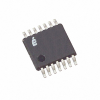
X9111TV14IZ-2.7 Intersil, X9111TV14IZ-2.7 Datasheet - Page 6

X9111TV14IZ-2.7
Manufacturer Part Number
X9111TV14IZ-2.7
Description
IC XDCP SGL 1024TAP 100K 14TSSOP
Manufacturer
Intersil
Series
XDCP™r
Datasheet
1.X9111TV14.pdf
(17 pages)
Specifications of X9111TV14IZ-2.7
Taps
1024
Resistance (ohms)
100K
Number Of Circuits
1
Temperature Coefficient
300 ppm/°C Typical
Memory Type
Non-Volatile
Interface
SPI, 3-Wire Serial
Voltage - Supply
2.7 V ~ 5.5 V
Operating Temperature
-40°C ~ 85°C
Mounting Type
Surface Mount
Package / Case
14-TSSOP
Resistance In Ohms
100K
Lead Free Status / RoHS Status
Lead free / RoHS Compliant
Available stocks
Company
Part Number
Manufacturer
Quantity
Price
Company:
Part Number:
X9111TV14IZ-2.7
Manufacturer:
TI
Quantity:
47
Five of the seven instructions are four bytes in length. These
instructions are:
• Read Wiper Counter Register – read the current wiper
• Write Wiper Counter Register – change current wiper
• Read Data Register – read the contents of the selected
• Write Data Register – write a new value to the selected
• Read Status – This command returns the contents of the
The basic sequence of the four byte instructions is illustrated
in Figure 3. These four-byte instructions exchange data
between the WCR and one of the Data Registers. A transfer
from a Data Register to a WCR is essentially a write to a
static RAM, with the static RAM controlling the wiper
position. The response of the wiper to this action will be
delayed by tWRL. A transfer from the WCR (current wiper
position), to a Data Register is a write to nonvolatile memory
and takes a minimum of tWR to complete. The transfer can
occur between the potentiometer and one of its associated
registers. The Read Status Register instruction is the only
unique format (see Figure 4).
Two instructions require a two-byte sequence to complete
(see Figure 2). These instructions transfer data between the
position of the selected pot,
position of the selected pot,
data register;
data register.
WIP bit which indicates if the internal write cycle is in
progress.
SCK
CS
SI
ID3 ID2 ID1 ID0 0
0
Device ID
FIGURE 3. FOUR-BYTE INSTRUCTION SEQUENCE (WRITE OR READ FOR WCR OR DATA REGISTERS)
SCK
1
CS
SI
0
1
0
Internal
Address
A1
6
ID3 ID2 ID1 ID0
A0 R/W I2
0
0
Device ID
1
Instruction
Opcode
FIGURE 2. TWO-BYTE INSTRUCTION SEQUENCE
I1 I0 0 RB RA
0
1
0
Address
Register
0
0
X X 0
Internal
Address
A1
0 0
A0
0
X9111
R/W
X X
I2
X X
host and the X9111; either between the host and one of the
Data Registers or directly between the host and the Wiper
Counter Register. These instructions are:
• XFR Data Register to Wiper Counter Register – This
• XFR Wiper Counter Register to Data Register – This
See Instruction format for more details.
Write in Process (WIP bit)
The contents of the Data Registers are saved to nonvolatile
memory when the CS pin goes from LOW to HIGH after a
complete write sequence is received by the device. The
progress of this internal write operation can be monitored by
a Write In Process bit (WIP). The WIP bit is read with a Read
Status command (see Figure 4).
Power Up and Down Requirements
There are no restrictions on the power-up condition of V
and the voltages applied to the potentiometer pins provided
that the V
voltages at R
are no restrictions on the power-down condition. However,
the datasheet parameters for the DCP do not apply until
1millisecond after V
Instruction
Opcode
transfers the contents of one specified Data Register to
the associated Wiper Counter Register.
transfers the contents of the specified Wiper Counter
Register to the specified associated Data Register.
I1
X
X
I0
CC
W
C
R
9
H
is always more positive than or equal to the
W
C
R
8
0
, R
W
C
R
7
Register
Address
L
RB
, and R
W
C
R
6
CC
Position
Wiper
W
C
R
5
RA
reaches its final value.
W
C
R
4
W
0
W
C
R
3
0
, i.e., V
W
C
R
2
0
0
W
C
R
1
CC
W
C
R
0
≥ R
H
, R
L
September 15, 2006
, R
W
. There
FN8159.4
CC


