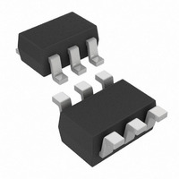
MCP4018T-502E/LT Microchip Technology, MCP4018T-502E/LT Datasheet - Page 38

MCP4018T-502E/LT
Manufacturer Part Number
MCP4018T-502E/LT
Description
IC DGTL POT 5K 128TAPS SC70-6
Manufacturer
Microchip Technology
Datasheet
1.MCP4018T-502ELT.pdf
(66 pages)
Specifications of MCP4018T-502E/LT
Taps
128
Resistance (ohms)
5K
Number Of Circuits
1
Temperature Coefficient
150 ppm/°C Typical
Memory Type
Volatile
Interface
I²C, 2-Wire Serial
Voltage - Supply
1.8 V ~ 5.5 V
Operating Temperature
-40°C ~ 125°C
Mounting Type
Surface Mount
Package / Case
SC-70-6, SC-88, SOT-363
Resistance In Ohms
5K
End To End Resistance
5kohm
Track Taper
Logarithmic
No. Of Steps
128
Resistance Tolerance
± 20%
Supply Voltage Range
1.8V To 5.5V
Control Interface
I2C
No. Of Pots
Single
Lead Free Status / RoHS Status
Lead free / RoHS Compliant
Other names
MCP4018T-502E/LTTR
Available stocks
Company
Part Number
Manufacturer
Quantity
Price
Company:
Part Number:
MCP4018T-502E/LT
Manufacturer:
Freescale
Quantity:
176
Part Number:
MCP4018T-502E/LT
Manufacturer:
MICROCHIP/微芯
Quantity:
20 000
MCP4017/18/19
5.4.1
The write operation requires the START condition,
Control Byte, Acknowledge, Data Byte, Acknowledge
and STOP (or RESTART) condition. The Control (Slave
Address) Byte requires the R/W bit equal to a logic zero
(R/W = “0”) to generate a write sequence. The
MCP4017/18/19 is responsible for generating the
Acknowledge (A) bits.
Data is written to the MCP4017/18/19 after every byte
transfer (during the A bit). If a STOP or RESTART
condition is generated during a data transfer (before
the A bit), the data will not be written to MCP4017/18/
19.
Data bytes may be written after each Acknowledge.
The command is terminated once a Stop (P) condition
occurs. Refer to
For a single byte write, the master sends a STOP or
RESTART condition after the 1st data byte is sent.
The MSb of each Data Byte is a don’t care, since the
wiper register is only 7-bits wide.
Figure 5-14
the Master Device and the MCP4017/18/19 device and
the resultant I
FIGURE 5-12:
DS22147A-page 38
Legend
S = Start Condition
P = Stop Condition
A = Acknowledge
X = Don’t Care
R/W = Read/Write bit
D6, D5, D4, D3, D2, D1, D0 = Data bits
S
WRITE OPERATION
shows the I
2
C bus values.
0 1 0
Figure 5-12
Slave Address Byte
Fixed
Address
I
x D6 D5 D4
2
2
C Write Command Format.
C communication behavior of
1
Data Byte
1
for the write sequence.
1 1
D3 D2 D1 D0
0
A
Read/Write bit (“0” = Write)
x D6 D5 D4
A
Data Byte
x D6 D5 D4
Data Byte
D3
5.4.2
The read operation requires the START condition,
Control Byte, Acknowledge, Data Byte, the master
generating the A and STOP condition. The Control
Byte requires the R/W bit equal to a logic one (R/W =
1) to generate a read sequence. The MCP4017/18/19
will A the Slave Address Byte and A all the Data Bytes.
The I
last Data Byte. If there are multiple Data Bytes, the I
Master will A all Data Bytes except the last Data Byte
(which it will A).
The MCP4017/18/19 maintains control of the SDA
signal until all data bits have been clocked out.
The command is terminated once a Stop (P) condition
occurs. Refer to
sequence. For a single read, the master sends a STOP
or RESTART condition after the 1st data byte (and A
bit) is sent from the slave.
Figure 5-14
the Master Device and the MCP4017/18/19 device and
the resultant I
D2 D1 D0 A
2
D3
C Master will A the Slave Address Byte and the
D2 D1 D0 A P
READ OPERATIONS
shows the I
2
C bus values.
x D6 D5 D4
Figure 5-13
Data Byte
STOP bit
2
© 2009 Microchip Technology Inc.
C communication behavior of
D3
for the read command
D2 D1 D0 A
2
C


