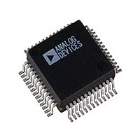
AD7339BS Analog Devices Inc, AD7339BS Datasheet

AD7339BS
Specifications of AD7339BS
Available stocks
Related parts for AD7339BS
AD7339BS Summary of contents
Page 1
FEATURES 8-Bit A/D Converter Two 8-Bit D/A Converters Two 8-Bit Serial D/A Converters Single +5 V Supply Operation On-Chip Reference Power-Down Mode 52-Lead PQFP Package GENERAL DESCRIPTION The AD7339 is a composite IC that contains both DAC and ADC ...
Page 2
AD7339–SPECIFICATIONS Parameter ADC Resolution Differential Nonlinearity Integral Nonlinearity Zero Input Offset Error Signal Range Full Power Input Bandwidth Conversion Rate Signal to (Noise + Distortion) Effective No. of Bits (ENOB) Intermodulation Distortion Error Rate Input Capacitance Coding PARALLEL DACS Resolution ...
Page 3
Parameter REFERENCE VREF Voltage VREFA/VREFB Voltage Load Capacitance I SINK I SOURCE LOGIC INPUTS V , Input High Voltage INH V , Input Low Voltage INL I , Input Leakage Current INH C , Input Capacitance IN LOGIC OUTPUTS V ...
Page 4
AD7339 TIMING CHARACTERISTICS Limit at Parameter T = – + ADC t 480 1 t 210 2 t 210 3 t 100 4 t 200 5 PARALLEL DACS t 430 6 t 200 7 t 200 ...
Page 5
SAMPLE N–2 SAMPLE N– ADCCLK D0 – D7 N–3 DACCLK DA0 – DA7 DB0 – DB7 DACA DACB t SCLK D1 SDATA LATCH SDAC0S SDAC1S REV. 0 SAMPLE N–2 N–1 Figure 3. ADC ...
Page 6
... Lead Temperature, Soldering Vapor Phase (60 sec +215 C Infrared (15 sec +220 C Model AD7339BS CAUTION ESD (electrostatic discharge) sensitive device. Electrostatic charges as high as 4000 V readily accumulate on the human body and test equipment and can discharge without detection. Although this device features proprietary ESD protection circuitry, permanent damage may occur on devices subjected to high energy electrostatic discharges ...
Page 7
Pin Number Mnemonic Power Supply 33 AVDD 2 DVDD1 12 DGND1 36 AGND1 22 DVDD2 29 DVDD3 21 DGND2 28 DGND3 32 AGND2 34 AGND3 ADCs 31 AIN 27 ADCCLK 26–23, 20–17 D0–D7 30 ADCPDB Parallel DACs 45–52 DA0–DA7 3–10 ...
Page 8
AD7339 Pin Number Mnemonic 11 DACPDB Serial DACs 16 SDATA 14 SCLK 15 LATCH 38 SDAC0S 37 SDAC0F 40 SDAC1S 39 SDAC1F 13 SDACPDB Reference 35 VREF 44, 42 VREFA/VREFB Function Digital Input. The parallel DACs, VREFA and VREFB, can ...
Page 9
FUNCTIONAL DESCRIPTION A-to-D Converter The A/D conversion circuitry consists of a track-and-hold ampli- fier followed by a flash A-to-D converter. Figure 6 shows the architecture of the ADC. AIN T/H DECODE COMPARATOR HOLD NETWORK LOGIC REFERENCE RESISTOR LADDER Figure 6. ...
Page 10
AD7339 The 4-bit offset nulling feature has a LSB size of 7.6 mV; thereby, allowing the user to vary the DAC output by 115 mV. Table I. Writing to the Parallel DACs Offset Registers ...
Page 11
TERMINOLOGY Differential Nonlinearity The difference between the measured and the ideal 1 LSB change between any two adjacent codes in the ADC or DACs. A speci- fied Differential Nonlinearity of 1 LSB max over the operating temperature range ensures monotonicity. ...
Page 12
AD7339 GROUNDING AND LAYOUT The printed circuit board that houses the AD7339 should be designed so that the analog and digital sections are separated and confined to certain areas of the board. This facilitates the use of ground planes that ...


