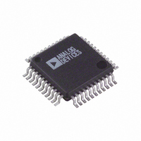
AD7891ASZ-1 Analog Devices Inc, AD7891ASZ-1 Datasheet - Page 4

AD7891ASZ-1
Manufacturer Part Number
AD7891ASZ-1
Description
IC DAS 12BIT 8CH HI-SPD 44-MQFP
Manufacturer
Analog Devices Inc
Type
Data Acquisition System (DAS)r
Datasheet
1.AD7891BSZ-2.pdf
(20 pages)
Specifications of AD7891ASZ-1
Resolution (bits)
12 b
Data Interface
Serial, Parallel
Sampling Rate (per Second)
500k
Voltage Supply Source
Single Supply
Voltage - Supply
5V
Operating Temperature
-40°C ~ 85°C
Mounting Type
Surface Mount
Package / Case
44-MQFP, 44-PQFP
Sampling Rate
450kSPS
Input Channel Type
Single Ended
Supply Voltage Range - Analog
4.75V To 5.25V
Supply Current
20mA
Number Of Elements
1
Resolution
12Bit
Sample Rate
454.5KSPS
Input Polarity
Bipolar
Input Type
Voltage
Rated Input Volt
±5/±10V
Differential Input
No
Power Supply Requirement
Single
Single Supply Voltage (typ)
5V
Single Supply Voltage (min)
4.75V
Single Supply Voltage (max)
5.25V
Dual Supply Voltage (typ)
Not RequiredV
Dual Supply Voltage (min)
Not RequiredV
Dual Supply Voltage (max)
Not RequiredV
Power Dissipation
100mW
Differential Linearity Error
±1LSB
Integral Nonlinearity Error
±1LSB
Operating Temp Range
-40C to 85C
Operating Temperature Classification
Industrial
Mounting
Surface Mount
Pin Count
44
Package Type
MQFP
Input Signal Type
Single-Ended
Lead Free Status / RoHS Status
Lead free / RoHS Compliant
Lead Free Status / RoHS Status
Lead free / RoHS Compliant, Lead free / RoHS Compliant
Available stocks
Company
Part Number
Manufacturer
Quantity
Price
Company:
Part Number:
AD7891ASZ-1
Manufacturer:
ADI
Quantity:
7
Company:
Part Number:
AD7891ASZ-1
Manufacturer:
Analog Devices Inc
Quantity:
10 000
Part Number:
AD7891ASZ-1
Manufacturer:
ADI/亚德诺
Quantity:
20 000
Company:
Part Number:
AD7891ASZ-1REEL
Manufacturer:
Analog Devices Inc
Quantity:
10 000
AD7891
TIMING CHARACTERISTICS
Parameter
t
Parallel Interface
Serial Interface
NOTES
1
2
3
4
Specifications subject to change without notice.
CONV
Sample tested during initial release and after any redesign or process change that may affect this parameter. All input signals are measured with tr = tf = 1 ns (10% to
90% of 5 V) and timed from a voltage level of 1.6 V.
See Figures 2, 3, and 4.
Measured with the load circuit of Figure 1 and defined as the time required for an output to cross 0.8 V or 2.4 V.
These times are derived from the measured time taken by the data outputs to change 0.5 V when loaded with the circuit of Figure 1. The measured number is then
extrapolated back to remove the effects of charging or discharging the 50 pF capacitor. This means that the times quoted in the timing characteristics are the true bus
relinquish times of the part and as such are independent of external bus loading capacitances.
t
t
t
t
t
t
t
t
t
t
t
t
t
t
t
t
t
t
t
t
t
t
t
1
2
3
4
5
6
7
8
9
11
13
14
17
18A
19
20
21
22
10
12
15
16
18
3
4
3
3
3
4
4
Figure 1. Load Circuit for Access Time and Bus Relinquish Time
A, B, Y Versions
1.6
0
35
25
5
0
35
55
35
25
5
30
30
20
25
25
5
15
20
0
30
0
30
20
15
10
30
1, 2
OUTPUT
PIN
TO
50pF
Unit
ms max
ns min
ns min
ns min
ns min
ns min
ns min
ns min
ns min
ns min
ns min
ns max
ns min
ns max
ns min
ns min
ns min
ns max
ns min
ns min
ns max
ns min
ns max
ns min
ns min
ns min
ns min
–4–
200 A
1.6mA
1.6V
Test Conditions/Comments
Conversion Time
CS to RD/WR Setup Time
Write Pulse Width
Data Valid to Write Setup Time
Data Valid to Write Hold Time
CS to RD/WR Hold Time
CONVST Pulse Width
EOC Pulse Width
Read Pulse Width
Data Access Time after Falling Edge of RD
Bus Relinquish Time after Rising Edge of RD
RFS Low to SCLK Falling Edge Setup Time
RFS Low to Data Valid Delay
SCLK High Pulse Width
SCLK Low Pulse Width
SCLK Rising Edge to Data Valid Hold Time
SCLK Rising Edge to Data Valid Delay
RFS to SCLK Falling Edge Hold Time
Bus Relinquish Time after Rising Edge of RFS
Bus Relinquish Time after Rising Edge of SCLK
TFS Low to SCLK Falling Edge Setup Time
Data Valid to SCLK Falling Edge Setup Time
Data Valid to SCLK Falling Edge Hold Time
TFS Low to SCLK Falling Edge Hold Time
REV. D


