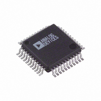
AD7891ASZ-1 Analog Devices Inc, AD7891ASZ-1 Datasheet - Page 2

AD7891ASZ-1
Manufacturer Part Number
AD7891ASZ-1
Description
IC DAS 12BIT 8CH HI-SPD 44-MQFP
Manufacturer
Analog Devices Inc
Type
Data Acquisition System (DAS)r
Datasheet
1.AD7891BSZ-2.pdf
(20 pages)
Specifications of AD7891ASZ-1
Resolution (bits)
12 b
Data Interface
Serial, Parallel
Sampling Rate (per Second)
500k
Voltage Supply Source
Single Supply
Voltage - Supply
5V
Operating Temperature
-40°C ~ 85°C
Mounting Type
Surface Mount
Package / Case
44-MQFP, 44-PQFP
Sampling Rate
450kSPS
Input Channel Type
Single Ended
Supply Voltage Range - Analog
4.75V To 5.25V
Supply Current
20mA
Number Of Elements
1
Resolution
12Bit
Sample Rate
454.5KSPS
Input Polarity
Bipolar
Input Type
Voltage
Rated Input Volt
±5/±10V
Differential Input
No
Power Supply Requirement
Single
Single Supply Voltage (typ)
5V
Single Supply Voltage (min)
4.75V
Single Supply Voltage (max)
5.25V
Dual Supply Voltage (typ)
Not RequiredV
Dual Supply Voltage (min)
Not RequiredV
Dual Supply Voltage (max)
Not RequiredV
Power Dissipation
100mW
Differential Linearity Error
±1LSB
Integral Nonlinearity Error
±1LSB
Operating Temp Range
-40C to 85C
Operating Temperature Classification
Industrial
Mounting
Surface Mount
Pin Count
44
Package Type
MQFP
Input Signal Type
Single-Ended
Lead Free Status / RoHS Status
Lead free / RoHS Compliant
Lead Free Status / RoHS Status
Lead free / RoHS Compliant, Lead free / RoHS Compliant
Available stocks
Company
Part Number
Manufacturer
Quantity
Price
Company:
Part Number:
AD7891ASZ-1
Manufacturer:
ADI
Quantity:
7
Company:
Part Number:
AD7891ASZ-1
Manufacturer:
Analog Devices Inc
Quantity:
10 000
Part Number:
AD7891ASZ-1
Manufacturer:
ADI/亚德诺
Quantity:
20 000
Company:
Part Number:
AD7891ASZ-1REEL
Manufacturer:
Analog Devices Inc
Quantity:
10 000
AD7891–SPECIFICATIONS
Parameter
DYNAMIC PERFORMANCE
DC ACCURACY
ANALOG INPUTS
REFERENCE INPUT/OUTPUT
LOGIC INPUTS
Signal-to-(Noise + Distortion) Ratio
Total Harmonic Distortion
Peak Harmonic or Spurious Noise
Intermodulation Distortion
Channel-to-Channel Isolation
Resolution
Minimum Resolution for which
Relative Accuracy
Differential Nonlinearity
Positive Full-Scale Error
Positive Full-Scale Error Match
Unipolar Offset Error
Unipolar Offset Error Match
Negative Full-Scale Error
Negative Full-Scale Error Match
Bipolar Zero Error
Bipolar Zero Error Match
AD7891-1 Input Voltage Range
AD7891-1 V
AD7891-1 V
AD7891-2 Input Voltage Range
AD7891-2 V
AD7891-2 V
REF IN Input Voltage Range
Input Impedance
Input Capacitance
REF OUT Output Voltage
REF OUT Error @ 25∞C
REF OUT Temperature Coefficient
REF OUT Output Impedance
Input High Voltage, V
Input Low Voltage, V
Input Current, I
Input Capacitance
@ 25∞C
T
Second-Order Terms
Third-Order Terms
No Missing Codes Are Guaranteed 12
T
MIN
MIN
to T
to T
MAX
MAX
INXA
INXA
INXA
INXA
INH
Input Resistance
Input Resistance
Input Resistance
Input Current
4
5
5
C
INL
IN
INH
4
4
4
5
4
4
2
5
4
4, 5
4, 5
4
4
A Version
70
70
–78
–80
–80
–80
–80
12
± 1
± 1
± 3
0.6
± 4
0.1
± 3
0.6
± 4
0.2
± 5
± 10
7.5
15
0 to 2.5
0 to 5
± 2.5
1.5
± 50
2.375/2.625 2.375/2.625 2.375/2.625 V min/V max
1.6
10
2.5
± 10
± 20
25
5
2.4
0.8
± 10
10
1
B Version
70
70
–78
–80
–80
–80
–80
12
12
± 0.75
± 1
± 3
0.6
± 4
0.1
± 3
0.6
± 4
0.2
± 5
± 10
7.5
15
0 to 2.5
0 to 5
± 2.5
1.5
± 50
1.6
10
2.5
± 10
± 20
25
5
2.4
0.8
± 10
10
(V
unless otherwise noted.)
DD
= 5 V
Y Version
70
70
–78
–80
–80
–80
–80
12
12
± 1
± 1
± 3
0.6
± 4
0.1
± 3
0.6
± 4
0.2
± 5
± 10
7.5
15
0 to 2.5
0 to 5
± 2.5
1.5
± 50
1.6
10
2.5
± 10
± 20
25
5
2.4
0.8
± 10
10
–2–
5%, AGND = DGND = 0 V, REF IN = 2.5 V. All specifications T
Unit
dB min
dB min
dB max
dB max
dB typ
dB typ
dB max
Bits
Bits
LSB max
LSB max
LSB max
LSB typ
LSB max
LSB typ
LSB max
LSB typ
LSB max
LSB typ
V
V
kW min
kW min
V
V
V
kW min
nA max
kW min
pF max
V nom
mV max
mV max
ppm/∞C typ
kW nom
V min
V max
mA max
pF max
1.5 LSB max.
Input ranges of 0 V to 2.5 V, 0 V to 5 V.
1 LSB max.
1.5 LSB max.
1.5 LSB max.
Input applied to both V
2.5 V ± 5%.
Test Conditions/Comments
Sample Rate = 454.5 kSPS
500 kSPS
fa = 9 kHz, fb = 9.5 kHz.
Any channel.
Input ranges of ± 2.5 V, ± 5 V, ± 10 V.
Input ranges of ± 2.5 V, ± 5 V, ± 10 V.
Input applied to both V
Input applied to V
Input range of ± 5 V.
Input range of ± 10 V.
Input applied to V
Input applied to V
Input ranges of ± 2.5 V and 0 V to 5 V.
Input range of 0 V to 2.5 V.
Resistor connected to internal reference node.
See REF IN input impedance.
V
V
DD
DD
= 5 V ± 5%.
= 5 V ± 5%.
3
(AD7891-2). Any channel.
INXA
INXA
INXA
, V
, V
, V
INXA
INXA
INXB
INXB
INXB
3
and V
and V
(AD7891-1),
= AGND.
= AGND.
= REF IN
INXB
INXB
MIN
to T
.
.
REV. D
6
.
MAX
,


