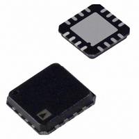
AD7879-1ACPZ-RL Analog Devices Inc, AD7879-1ACPZ-RL Datasheet - Page 22

AD7879-1ACPZ-RL
Manufacturer Part Number
AD7879-1ACPZ-RL
Description
IC ADC 12BIT CTLR TOUCH 16LFCSP
Manufacturer
Analog Devices Inc
Type
Resistiver
Specifications of AD7879-1ACPZ-RL
Resolution (bits)
12 b
Data Interface
I²C, Serial
Touch Panel Interface
4-Wire
Number Of Inputs/keys
1 TSC
Data Rate/sampling Rate (sps, Bps)
105k
Voltage Reference
External
Voltage - Supply
1.6 V ~ 3.6 V
Current - Supply
10nA
Operating Temperature
-40°C ~ 85°C
Mounting Type
Surface Mount
Package / Case
16-LFCSP
Voltage Supply Source
Single Supply
Sampling Rate (per Second)
105k
Sampling Rate
105kSPS
Supply Voltage Range - Analog
1.6V To 3.6V
Supply Current
480µA
Digital Ic Case Style
CSP
No. Of Pins
16
Lead Free Status / RoHS Status
Lead free / RoHS Compliant
AD7879/AD7889
DETAILED REGISTER DESCRIPTIONS
All addresses and default values are expressed in hexadecimal.
Table 12. Control Register 1
Address
0x01
1
2
If GPIO is enabled in Control Register 2 (Bit 13), AUX and VBAT are both ignored. If AUX and VBAT are both selected in Control Register 3 and GPIO is disabled, AUX is
ignored and VBAT is measured.
Note that these bits are cleared to 00 at the end of the conversion sequence if the conversion interval timer bits in Control Register 1 (Address 0x01) Bits[7:0] = 0x00 at
the end of the conversion sequence.
Bit Name
Disable PENIRQ
CHNL ADD[2:0]
ADC MODE[1:0]
ACQ[1:0]
TMR[7:0]
Data Bit
15
[14:12]
[11:10]
[9:8]
[7:0]
Description
Pen interrupt enable.
0 = PENIRQ is enabled.
1 = PENIRQ is disabled and INT is enabled.
ADC channel address for manual conversion (ADC mode = 01).
111 = X+ input (Y position).
110 = Y+ input (X position).
101 = X+ (Z1) input for touch-pressure calculation.
100 = Y− (Z2) input (used for touch-pressure measurement).
011 = AUX input.
010 = VBAT input.
001 = temperature measurement.
000 = not applicable.
ADC mode.
00 = no conversion.
01 = single conversion.
10 = conversion sequence (slave mode).
11 = conversion sequence (master mode).
ADC acquisition time.
00 = 4 clock periods (2 µs).
01 = 8 clock periods (4 µs).
10 = 16 clock periods (8 µs).
11 = 32 clock periods (16 µs).
Note that the acquisition time does not apply to the temperature sensor channels;
the temperature channel has a constant settling time of 16 μs.
Conversion interval timer.
Starts at 550 µs (00000001) and continues to 9.440 ms (11111111) in steps of 35 µs
(see Table 18).
Note that, in slave mode, the conversion interval timer starts to count as soon as the
conversion sequence is finished; in master mode, it starts to count again only if the
screen remains touched. If the screen is released, the timer stops counting and, on
the next screen touch, a conversion starts immediately.
1
Rev. C | Page 22 of 40
1
2
2
Default
Value
0x0000


