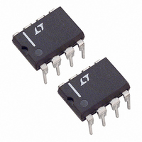
LTC1291CCN8 Linear Technology, LTC1291CCN8 Datasheet - Page 9

LTC1291CCN8
Manufacturer Part Number
LTC1291CCN8
Description
IC DATA ACQ SYSTEM 12BIT 8-DIP
Manufacturer
Linear Technology
Type
Data Acquisition System (DAS)r
Datasheet
1.LTC1291DCN8PBF.pdf
(20 pages)
Specifications of LTC1291CCN8
Resolution (bits)
12 b
Data Interface
Serial, Parallel
Voltage Supply Source
Single Supply
Voltage - Supply
5V
Operating Temperature
0°C ~ 70°C
Mounting Type
Through Hole
Package / Case
8-DIP (0.300", 7.62mm)
Lead Free Status / RoHS Status
Contains lead / RoHS non-compliant
Sampling Rate (per Second)
-
Available stocks
Company
Part Number
Manufacturer
Quantity
Price
Part Number:
LTC1291CCN8
Manufacturer:
LT
Quantity:
20 000
Company:
Part Number:
LTC1291CCN8#PBF
Manufacturer:
Linear Technology
Quantity:
135
Input Data Word
The 4-bit data word is clocked into the D
edge of the clock after chip select goes low and the start
bit has been recognized. Further inputs on the D
then ignored until the next CS cycle. The input word is
defined as follows:
Start Bit
The first “logical one” clocked into the D
goes low is the start bit. The start bit initiates the data
transfer and all leading zeroes which precede this logical
one will be ignored. After the start bit is received, the
remaining bits of the input word will be clocked in. Further
inputs on the D
cycle.
MUX Address
The bits of the input word following the START BIT assign
the MUX configuration for the requested conversion. For
a given channel selection, the converter will measure the
voltage between the two channels indicated by the “+” and
“–” signs in the selected row of the following table. In
single-ended mode, all input channels are measured with
respect to GND. Only the “+” inputs have sample-and-
holds. Signals applied at the “–” inputs must not change
more than the required accuracy during the conversion.
A
PPLICATI
START
IN
O
Figure 2. Input Data Word
pin are then ignored until the next CS
SGL/
DIFF
U
MUX ADDRESS
S
I FOR ATIO
ODD/
SIGN
U
MSB-FIRST/
LSB-FIRST
MSBF
W
IN
SHUTDOWN
IN
pin on the rising
POWER
PS
input after CS
1291 F02
IN
U
pin are
MSB-First/LSB-First (MSBF)
The output data of the LTC1291 is programmed for MSB-
first or LSB-first sequence using the MSBF bit. When the
MSBF bit is a logical one, data will appear on the D
in MSB-first format. Logical zeroes will be filled in indefi-
nitely following the last data bit to accommodate longer
word lengths required by some microprocessors. When
the MSBF bit is a logical zero, LSB-first data will follow the
normal MSB-first data on the D
Sequence).
Power Shutdown
The power shutdown feature of the LTC1291 is activated
by making the PS bit a logical zero. If CS remains low after
the PS bit has been received, a 12-bit D
logical ones will be shifted out followed by logical zeroes
until CS goes high. Then the D
impedance state. The LTC1291 will remain in the shut-
down mode until the next CS cycle. There is no warm-up
or wait period required after coming out of the power
shutdown cycle so a conversion can commence after CS
goes low (see Power Shutdown Operating Sequence).
SGL/DIFF ODD/SIGN
1
1
0
0
MUX ADDRESS
Multiplexer Channel Selection
0
1
0
1
0
+
+
–
CHANNEL #
OUT
OUT
line will go into its high
line (see Operating
1
+
–
+
OUT
LTC1291
word with all
GND
–
–
OUT
1291fa
9
line


