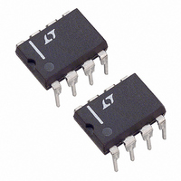
LTC1291CCN8 Linear Technology, LTC1291CCN8 Datasheet - Page 12

LTC1291CCN8
Manufacturer Part Number
LTC1291CCN8
Description
IC DATA ACQ SYSTEM 12BIT 8-DIP
Manufacturer
Linear Technology
Type
Data Acquisition System (DAS)r
Datasheet
1.LTC1291DCN8PBF.pdf
(20 pages)
Specifications of LTC1291CCN8
Resolution (bits)
12 b
Data Interface
Serial, Parallel
Voltage Supply Source
Single Supply
Voltage - Supply
5V
Operating Temperature
0°C ~ 70°C
Mounting Type
Through Hole
Package / Case
8-DIP (0.300", 7.62mm)
Lead Free Status / RoHS Status
Contains lead / RoHS non-compliant
Sampling Rate (per Second)
-
Available stocks
Company
Part Number
Manufacturer
Quantity
Price
Part Number:
LTC1291CCN8
Manufacturer:
LT
Quantity:
20 000
Company:
Part Number:
LTC1291CCN8#PBF
Manufacturer:
Linear Technology
Quantity:
135
LTC1291
Interfacing to the Parallel Port of the Intel 8051 Family
The Intel 8051 has been chosen to show the interface
between the LTC1291 and parallel port microprocessors.
Usually the signals CS, D
port lines and the D
LABEL MNEMONIC
A
WAIT1 BPL
WAIT2 LDAA
12
PPLICATI
LDAA
LDAA
STAA
BPL
LDAA
STAA
LDAA
R2
R1
(D
IN
MSB
B11
B3
/D
DATA
OUT
D OUT FROM LTC1291 STORED IN 8051 RAM
CLK
CS
)
B10
B2
O
OPERAND
$1029
WAIT1
$51
$102A
$1029
WAIT2
$102A
$62
$52
OUT
U
B9
B1
CLK BEFORE THE 5TH FALLING CLK
S
signal is read on a fourth port line.
AS INPUT AFTER THE 5TH RISING
IN
START
LSB
I FOR ATIO
1
B8
and CLK are generated on three
B0
U
8051 P1.2 OUTPUT DATA
8051 P1.2 RECONFIGURED
COMMENTS
CHECK SPI STATUS REG
CHECK IF TRANSFER IS DONE
LOAD DIN INTO ACC A FROM $51
LOAD DIN INTO SPI, START SCK
CHECK SPI STATUS REG
CHECK IF TRANSFER IS DONE
LOAD LTC1291 MSBs INTO ACC A
STORE MSBs IN $62
LOAD DUMMY DIN INTO ACC A
FROM $52
ODD/
SIGN
B7
0
TO LTC1291
2
B6
0
W
SGL/
DIFF
Hardware and Software Interface to Intel 8051
3
Timing Diagram for Interface to Intel 8051
B5
0
MSBF
B4
4
0
U
PS
PS BIT LATCHED
INTO LTC1291
5
ANALOG
INPUTS
B11
LABEL MNEMONIC
WAIT3 LDAA
LTC1291 TAKES CONTROL OF DATA
LINE ON 5TH FALLING CLK
This works very well. One can save a line by tying the D
and D
and MUX Address to the LTC1291 over the line connected
to P1.2. Then P1.2 is reconfigured as an input and the 8051
reads back the 12-bit A/D result over the same data line.
B10 B9 B8 B7 B6 B5 B4
CH0
CH1
LTC1291 SENDS A/D RESULT
LTC1291
OUT
STAA
BPL
BSET
LDAA
STAA
JMP
BACK TO 8051 P1.2
lines together. The 8051 first sends the start bit
D
CLK
OUT
D
CS
IN
MUX ADDRESS
$102A
WAIT3
$63
OPERAND
$1029
$08,X#$01
$102A
LOOP
A/D RESULT
B3 B2
P1.3
P1.2
P1.4
LOAD DUMMY DIN INTO SPI,
START SCK
CHECK SPI STATUS REG
CHECK IF TRANSFER IS DONE
D0 GOES HIGH (CS GOES HIGH)
LOAD LTC1291 LSBs IN ACC
STORE LSBs IN $63
START NEXT CONVERSION
COMMENTS
B1
8051
B0
LTC1291 AI08
LTC1291 AI09
1291fa
IN


