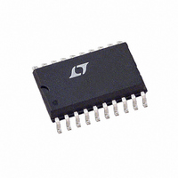
LTC1290BCSW#TRPBF Linear Technology, LTC1290BCSW#TRPBF Datasheet - Page 7

LTC1290BCSW#TRPBF
Manufacturer Part Number
LTC1290BCSW#TRPBF
Description
IC DATA ACQ SYS 12BIT 20-SOIC
Manufacturer
Linear Technology
Type
Data Acquisition System (DAS), ADCr
Datasheet
1.LTC1290CCSWPBF.pdf
(32 pages)
Specifications of LTC1290BCSW#TRPBF
Resolution (bits)
12 b
Sampling Rate (per Second)
50k
Data Interface
Serial, Parallel
Voltage Supply Source
Dual ±
Voltage - Supply
±5V
Operating Temperature
0°C ~ 70°C
Mounting Type
Surface Mount
Package / Case
20-SOIC (7.5mm Width)
Lead Free Status / RoHS Status
Lead free / RoHS Compliant
Available stocks
Company
Part Number
Manufacturer
Quantity
Price
** MAXIMUM R
PI FU CTIO S
CH0 to CH7 (Pin 1 to Pin 8): Analog Inputs. The analog
inputs must be free of noise with respect to AGND.
COM (Pin 9): Common. The common pin defines the zero
reference point for all single-ended inputs. It must be free
of noise and is usually tied to the analog ground plane.
DGND (Pin 10): Digital Ground. This is the ground for the
internal logic. Tie to the ground plane.
AGND (Pin 11): Analog Ground. AGND should be tied
directly to the analog ground plane.
TYPICAL PERFOR A CE CHARACTERISTICS
VALUE AT WHICH A 0.1LSB CHANGE IN FULL-SCALE
ERROR FROM ITS VALUE AT R
100
10k
1.0
200
180
160
140
120
100
1k
10
U
80
60
40
20
10
Maximum Filter Resistor vs
Cycle Time
0
Supply Current (Power Shutdown)
vs ACLK
V
CMOS LEVELS
CC
= 5V
FILTER
U
1.00
ACLK FREQUENCY (MHz)
CYCLE TIME, t
100
REPRESENTS THE FILTER RESISTOR
V
C
IN
FILTER
2.00
R
U
FILTER
FILTER
≥ 1µF
CYC
1000
(µs)
= 0 IS FIRST DETECTED.
3.00
W
1290 • TPC10
1290 • TPC13
+
–
10000
U
4.00
1000
100
900
800
700
600
500
400
300
200
100
10
1
0
100
–50
Sample-and-Hold Acquisition
Time vs Source Resistance
Input Channel Leakage Current
vs Temperature
V
V
T
0V TO 5V INPUT STEP
V
REF
CC
A
–30
IN
= 25°C
= 5V
AMBIENT TEMPERATURE, T
R
= 5V
SOURCE
–10
10
+
+
–
R
SOURCE
30
1k
OFF CHANNEL
V
potential in the circuit. (Ground in single supply applica-
tions.)
REF
ence inputs must be kept free of noise with respect to
AGND.
CS (Pin 15): Chip Select Input. A logic low on this input
enables data transfer.
D
result is shifted out of this output.
50
+ (Ω)
OUT
–
(Pin 12): Negative Supply. Tie V
GUARANTEED
ON CHANNEL
70
–
, REF
(Pin 16): Digital Data Output. The A/D conversion
A
90 110
(°C)
LTC1290 • TPC11
1290 • TPC14
+
(Pins 13, 14): Reference Inputs. The refer-
10k
130
2.25
2.00
1.75
1.50
1.25
1.00
0.50
0.75
0.25
10
0
9
8
7
6
5
4
3
2
1
0
–50
0
Supply Current (Power Shutdown)
vs Temperature
Noise Error vs Reference Voltage
ACLK OFF DURING
POWER SHUTDOWN
LTC1290 NOISE 200µV
–30
AMBIENT TEMPERATURE, T
REFERENCE VOLTAGE, V
–10
1
10
–
2
30
to most negative
LTC1290
50
P-P
3
70
REF
A
90 110
(V)
(°C)
4
1290 • TPC15
1290 • TPC12
1290fe
7
130
5


