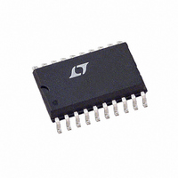
LTC1290BCSW#TRPBF Linear Technology, LTC1290BCSW#TRPBF Datasheet - Page 26

LTC1290BCSW#TRPBF
Manufacturer Part Number
LTC1290BCSW#TRPBF
Description
IC DATA ACQ SYS 12BIT 20-SOIC
Manufacturer
Linear Technology
Type
Data Acquisition System (DAS), ADCr
Datasheet
1.LTC1290CCSWPBF.pdf
(32 pages)
Specifications of LTC1290BCSW#TRPBF
Resolution (bits)
12 b
Sampling Rate (per Second)
50k
Data Interface
Serial, Parallel
Voltage Supply Source
Dual ±
Voltage - Supply
±5V
Operating Temperature
0°C ~ 70°C
Mounting Type
Surface Mount
Package / Case
20-SOIC (7.5mm Width)
Lead Free Status / RoHS Status
Lead free / RoHS Compliant
Available stocks
Company
Part Number
Manufacturer
Quantity
Price
LTC1290
A “Quick Look” Circuit for the LTC1290
Users can get a quick look at the function and timing of the
LTC1290 by using the following simple circuit. REF
D
single-ended input, unipolar mode, MSB-first format and
16-bit word length. ACLK and SCLK are tied together and
driven by an external clock. CS is driven at 1/128 the clock
rate by the CD4520 and D
pins are tied to a ground plane. The output data from the
D
to trigger on the falling edge of CS.
26
TYPICAL
IN
OUT
are tied to V
pin can be viewed on an oscilloscope which is set up
A
PPLICATI
CC
selecting a 5V input span, CH7 as a
OUT
outputs the data. All other
O
U
ACLK/
SCLK
D
S
CS
OUT
Scope Trace of LTC1290 “Quick Look” Circuit
Showing A/D Output of 010101010101 (555
DEGLITCHER
TIME
+
and
VERTICAL: 5V/DIV
HORIZONTAL: 1µs/DIV
(B11)
MSB
V
IN
22µF
LSB
(B0)
CHO
CH1
CH2
CH3
CH4
CH5
CH6
CH7
COM
DGND
LTC1290
A “Quick Look” Circuit for the LTC1290
AGND
ACLK
SCLK
D
REF
REF
V
OUT
D
ZEROS
HEX
CS
V
FILLS
CC
IN
+
–
–
)
OSCILLOSCOPE
TO
f
f/128
CLOCK IN
2MHz MAX
CLK
EN
Q1
Q2
Q3
Q4
RESET
V
SS
CD4520
RESET
V
CLK
DD
Q4
Q3
Q2
Q1
EN
5V
0.1µF
1290fe
1290 TA02


