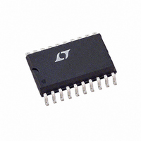
LTC1290BCSW#TR Linear Technology, LTC1290BCSW#TR Datasheet - Page 24

LTC1290BCSW#TR
Manufacturer Part Number
LTC1290BCSW#TR
Description
IC DATA ACQ SYS 12BIT 5V 20SOIC
Manufacturer
Linear Technology
Type
Data Acquisition System (DAS), ADCr
Datasheet
1.LTC1290CCSWPBF.pdf
(32 pages)
Specifications of LTC1290BCSW#TR
Resolution (bits)
12 b
Sampling Rate (per Second)
50k
Data Interface
Serial, Parallel
Voltage Supply Source
Dual ±
Voltage - Supply
±5V
Operating Temperature
0°C ~ 70°C
Mounting Type
Surface Mount
Package / Case
20-SOIC (7.5mm Width)
Lead Free Status / RoHS Status
Contains lead / RoHS non-compliant
Available stocks
Company
Part Number
Manufacturer
Quantity
Price
LTC1290
8. Overvoltage Protection
Applying signals to the analog MUX that exceed the
positive or negative supply of the device will degrade the
accuracy of the A/D and possibly damage the device. For
example this condition would occur if a signal is applied to
the analog MUX before power is applied to the LTC1290.
Another example is the input source is operating from
different supplies of larger value than the LTC1290. These
conditions should be prevented either with proper supply
sequencing or by use of external circuitry to clamp or
current limit the input source. As shown in Figure 20, a 1k
resistor is enough to stand off ±15V (15mA for one only
channel). If more than one channel exceeds the supplies
24
A
PPLICATI
Figure 18. LTC1290 ENOB vs Input Frequency
–100
–120
–140
–20
–40
–60
–80
11.6
11.2
10.8
10.4
9.6
9.2
8.8
0
12
10
0
0
Figure 17a. LTC1290 FFT Plot
O
4
U
20
S
8
FREQUENCY (kHz)
FREQUENCY (kHz)
40
I FOR ATIO
12
U
f
SNR = 73.25dB
f
IN
SAMPLE
f
16
SAMPLE
60
= 1kHz
20
= 50.6kHz
W
= 50.6kHz
80
1290 • F17a
24
1290 F18
100
U
then the following guidelines can be used. Limit the
current to 7mA per channel and 28mA for all channels.
This means four channels can handle 7mA of input current
each. Reducing the ACLK and SCLK frequencies from the
maximum of 4MHz and 2MHz, respectively, (see Typical
Performance Characteristics curves Maximum ACLK Fre-
quency vs Source Resistance and Sample-and-Hold
Acquisition Time vs Source Resistance) allows the use of
larger current limiting resistors. Use 1N4148 diode clamps
from the MUX inputs to V
resistor will not allow the maximum clock speeds to be
used or if an unknown source is used to drive the LTC1290
MUX inputs.
–100
–120
–140
–20
–40
–60
–80
–100
–120
–20
–40
–60
–80
0
0
0
0
f
SNR = 72.54dB
f
IN
SAMPLE
Figure 17b. LTC1290 FFT Plot
= 25kHz
Figure 19. LTC1290 FFT Plot
4
4
= 50.6kHz
8
FREQUENCY (kHz)
8
FREQUENCY (kHz)
CC
12
12
and V
16
f
f
f
IN1
IN2
SAMPLE
16
–
= 5.1kHz
= 5.6kHz
if the value of the series
20
20
= 50.6kHz
1290 • F17b
24
1290 • F19
24
1290fe


