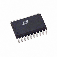
LTC1290BCSW#TR Linear Technology, LTC1290BCSW#TR Datasheet - Page 22

LTC1290BCSW#TR
Manufacturer Part Number
LTC1290BCSW#TR
Description
IC DATA ACQ SYS 12BIT 5V 20SOIC
Manufacturer
Linear Technology
Type
Data Acquisition System (DAS), ADCr
Datasheet
1.LTC1290CCSWPBF.pdf
(32 pages)
Specifications of LTC1290BCSW#TR
Resolution (bits)
12 b
Sampling Rate (per Second)
50k
Data Interface
Serial, Parallel
Voltage Supply Source
Dual ±
Voltage - Supply
±5V
Operating Temperature
0°C ~ 70°C
Mounting Type
Surface Mount
Package / Case
20-SOIC (7.5mm Width)
Lead Free Status / RoHS Status
Contains lead / RoHS non-compliant
Available stocks
Company
Part Number
Manufacturer
Quantity
Price
LTC1290
Differential Inputs
With differential inputs or when the COM pin is not tied to
ground, the A/D no longer converts just a single voltage but
rather the difference between two voltages. In these cases,
the voltage on the selected “+” input is still sampled and held
and therefore may be rapidly time varying just as in single-
ended mode. However, the voltage on the selected “–” input
must remain constant and be free of noise and ripple
throughout the conversion time. Otherwise, the differencing
operation may not be performed accurately. The conversion
time is 52 ACLK cycles. Therefore, a change in the “–” input
voltage during this interval can cause conversion errors.
For a sinusoidal voltage on the “–” input this error would be:
Where f(“–”) is the frequency of the “–” input voltage,
V
the ACLK. In most cases V
a 60Hz signal on the “–” input to generate a 0.25LSB error
(300µV) with the converter running at ACLK = 4MHz, its
peak value would have to be 61mV.
5. Reference Inputs
The voltage between the reference inputs of the LTC1290
defines the voltage span of the A/D converter. The refer-
ence inputs will have transient capacitive switching cur-
rents due to the switched capacitor conversion technique
(see Figure 14). During each bit test of the conversion
(every 4 ACLK cycles), a capacitive current spike will be
generated on the reference pins by the A/D. These current
spikes settle quickly and do not cause a problem. How-
ever, if slow settling circuitry is used to drive the reference
inputs, care must be taken to insure that transients caused
by these current spikes settle completely during each bit
test of the conversion.
22
A
PEAK
PPLICATI
V
ERROR (MAX)
is its peak amplitude and f
Figure 14. Reference Input Equivalent Circuit
R
V
OUT
REF
= (V
O
REF+
REF–
13
14
U
PEAK
S
)(2π)[ f(“–”)](52/f
ERROR
I FOR ATIO
U
will not be significant. For
EVERY 4 ACLK CYCLES
R
ACLK
ON
W
is the frequency of
8pF TO 40pF
LTC1290
ACLK
LTC 1290 F14
)
U
When driving the reference inputs, two things should be
kept in mind:
1. Transients on the reference inputs caused by the
2. It is recommended that REF
capacitive switching currents must settle completely
during each bit test (each 4 ACLK cycles). Figures 15
and 16 show examples of both adequate and poor
settling. Using a slower ACLK will allow more time for
the reference to settle. However, even at the maximum
ACLK rate of 4MHz most references and op amps can
be made to settle within the 1µs bit time. For example
the LT1236 will settle adequately.
the analog ground plane. If REF
other than ground, the voltage must not change during
a conversion cycle. This voltage must also be free of
noise and ripple with respect to analog ground.
Figure 16. Poor Reference Settling Can Cause A/D Errors
Figure 15. Adequate Reference Settling
HORIZONTAL: 1µs/DIV
HORIZONTAL: 1µs/DIV
–
input be tied directly to
–
is biased at a voltage
1290fe


