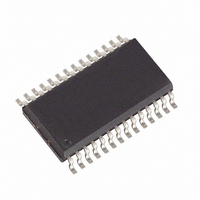
MAX196BCWI+ Maxim Integrated Products, MAX196BCWI+ Datasheet - Page 14

MAX196BCWI+
Manufacturer Part Number
MAX196BCWI+
Description
IC DAS 12BIT 6CH 28-SOIC
Manufacturer
Maxim Integrated Products
Type
Data Acquisition System (DAS)r
Datasheet
1.MAX196BCAI.pdf
(16 pages)
Specifications of MAX196BCWI+
Resolution (bits)
12 b
Sampling Rate (per Second)
100k
Data Interface
Parallel
Voltage Supply Source
Single Supply
Voltage - Supply
4.75 V ~ 5.25 V
Operating Temperature
0°C ~ 70°C
Mounting Type
Surface Mount
Package / Case
28-SOIC (7.5mm Width)
Lead Free Status / RoHS Status
Lead free / RoHS Compliant
results may be read. Input overvoltage protection is
active in all power-down modes. The device returns to
normal operation on the first WR falling edge during
write operation.
The bandgap reference and reference buffer remain
active in STBYPD mode, maintaining the voltage on the
4.7µF capacitor at the REF pin. This is a “DC” state that
does not degrade after power-down of any duration.
Therefore, you can use any sampling rate with this
mode, without regard to start-up delays.
However, in FULLPD mode, only the bandgap refer-
ence is active. Connect a 33µF capacitor between REF
and AGND to maintain the reference voltage between
conversions and to reduce transients when the buffer is
enabled and disabled. Throughput rates down to 1ksps
can be achieved without allotting extra acquisition time
for reference recovery prior to conversion. This allows
conversion to begin immediately after power-down
ends. If the discharge of the REF capacitor during
FULLPD exceeds the desired limits for accuracy (less
Multirange, Single +5V, 12-Bit DAS
with 12-Bit Bus Interface
Figure 10. Unipolar Transfer Function
14
00... 011
00... 010
00... 001
00... 000
11... 111
11... 110
11... 101
OUTPUT CODE
______________________________________________________________________________________
0
1
2
3
INPUT VOLTAGE (LSB)
Choosing Power-Down Modes
FULL-SCALE
TRANSITION
FS -
3
/
2
LSB
1 LSB =
FS
4096
FS
than a fraction of an LSB), run a STBYPD power-down
cycle prior to starting conversions. Take into account
that the reference buffer recharges the bypass capaci-
tor at an 80mV/ms slew rate, and add 50µs for settling
time. Throughput rates of 10ksps offer typical supply
currents of 470µA, using the recommended 33µF
capacitor value.
Selecting STBYPD on every conversion automatically
shuts the MAX196/MAX198 down after each conversion
without requiring any start-up time on the next conversion.
Output data coding for the MAX196/MAX198 is binary
in unipolar mode with 1LSB = (FS / 4096) and twos-
complement binary in bipolar mode with 1LSB = [(2 x
|
successive-integer LSB values. Figures 10 and 11
show the input/output (I/O) transfer functions for unipo-
lar and bipolar operations, respectively. For full-scale
(FS) values, refer to Table 1.
Figure 11. Bipolar Transfer Function
FS
011... 111
011... 110
000... 001
000... 000
111... 111
100... 010
100... 001
100... 000
|
) / 4096]. Code transitions occur halfway between
OUTPUT CODE
-FS
INPUT VOLTAGE (LSB)
0V
Transfer Function
Auto-Shutdown
+FS - 1 LSB
1 LSB =
2 FS
4096


