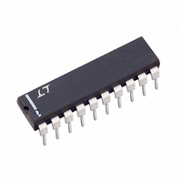
LTC1290CCN#PBF Linear Technology, LTC1290CCN#PBF Datasheet - Page 23

LTC1290CCN#PBF
Manufacturer Part Number
LTC1290CCN#PBF
Description
IC DATA ACQ SYS 12BIT 20-DIP
Manufacturer
Linear Technology
Type
Data Acquisition System (DAS), ADCr
Datasheet
1.LTC1290CCSWPBF.pdf
(32 pages)
Specifications of LTC1290CCN#PBF
Resolution (bits)
12 b
Sampling Rate (per Second)
50k
Data Interface
Serial, Parallel
Voltage Supply Source
Dual ±
Voltage - Supply
±5V
Operating Temperature
0°C ~ 70°C
Mounting Type
Through Hole
Package / Case
20-DIP (0.300", 7.62mm)
Lead Free Status / RoHS Status
Lead free / RoHS Compliant
Available stocks
Company
Part Number
Manufacturer
Quantity
Price
6. Reduced Reference Operation
The effective resolution of the LTC1290 can be increased
by reducing the input span of the converter. The LTC1290
exhibits good linearity and gain over a wide range of
reference voltages (see the typical curves of Linearity and
Gain Error vs Reference Voltage). However, care must be
taken when operating at low values of V
reduced LSB step size and the resulting higher accuracy
requirement placed on the converter. The following factors
must be considered when operating at low V
Offset with Reduced V
The offset of the LTC1290 has a larger effect on the output
code when the A/D is operated with reduced reference
voltage. The offset (which is typically a fixed voltage)
becomes a larger fraction of an LSB as the size of the LSB
is reduced. The typical curve of Unadjusted Offset Error vs
Reference Voltage shows how offset in LSBs is related to
reference voltage for a typical value of V
a V
becomes 0.4LSB with a 1.25V reference. If this offset is
unacceptable, it can be corrected digitally by the receiving
system or by offsetting the “–” input to the LTC1290.
Noise with Reduced V
The total input referred noise of the LTC1290 can be
reduced to approximately 200µV peak-to-peak using a
ground plane, good bypassing, good layout techniques
and minimizing noise on the reference inputs. This noise
is insignificant with a 5V reference but will become a larger
fraction of an LSB as the size of the LSB is reduced. The
typical curve of Noise Error vs Reference Voltage shows
the LSB contribution of this 200µV of noise.
For operation with a 5V reference, the 200µV noise is only
0.16LSB peak-to-peak. In this case, the LTC1290 noise
will contribute virtually no uncertainty to the output code.
However, for reduced references, the noise may become
a significant fraction of an LSB and cause undesirable jitter
in the output code. For example, with a 1.25V reference,
this same 200µV noise is 0.64LSB peak-to-peak. This will
A
PPLICATI
1. Offset
2. Noise
OS
of 0.1mV which is 0.1LSB with a 5V reference
O
U
REF
REF
S
I FOR ATIO
U
W
REF
OS
because of the
. For example,
REF
U
values:
reduce the range of input voltages over which a stable
output code can be achieved by 0.64LSB. In this case
averaging readings may be necessary.
This noise data was taken in a very clean setup. Any setup in-
duced noise (noise or ripple on V
the internal noise. The lower the reference voltage to be used,
the more critical it becomes to have a clean, noise-free setup.
7. LTC1290 AC Characteristics
Two commonly used figures of merit for specifying the
dynamic performance of the A/D’s in digital signal process-
ing applications are the Signal-to-Noise Ratio (SNR) and
the “effective number of bits (ENOB).” SNR is defined as
the ratio of the RMS magnitude of the fundamental to the
RMS magnitude of all the nonfundamental signals up to the
Nyquist frequency (half the sampling frequency). The
theoretical maximum SNR for a sine wave input is given by:
where N is the number of bits. Thus the SNR is a function
of the resolution of the A/D. For an ideal 12-bit A/D the SNR
is equal to 74dB. A Fast Fourier Transform(FFT) plot of the
output spectrum of the LTC1290 is shown in Figures 17a
and 17b. The input (f
with the sampling frequency (f
obtained from the plot are 73.25dB and 72.54dB.
Rewriting the SNR expression it is possible to obtain the
equivalent resolution based on the SNR measurement.
This is the so-called effective number of bits (ENOB). For
the example shown in Figures 17a and 17b, N = 11.9 bits
and 11.8 bits, respectively. Figure 18 shows a plot of ENOB
as a function of input frequency. The curve shows the
A/D’s ENOB remain in the range of 11.9 to 11.8 for input
frequencies up to f
Figure 19 shows an FFT plot of the output spectrum for two
tones applied to the input of the A/D. Nonlinearities in the
A/D will cause distortion products at the sum and differ-
ence frequencies of the fundamentals and products of the
fundamentals. This is classically referred to as intermod-
ulation distortion (IMD).
SNR = (6.02N + 1.76dB)
N = (SNR – 1.76dB)/6.02
S
/2.
IN
) frequencies are 1kHz and 25kHz
CC
, V
S
) at 50.6kHz. The SNR
REF
, V
IN
LTC1290
or V
–
) will add to
23
1290fe


