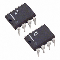
LTC1297DCN8 Linear Technology, LTC1297DCN8 Datasheet - Page 22

LTC1297DCN8
Manufacturer Part Number
LTC1297DCN8
Description
IC DATA ACQ SYSTEM 12BIT 8-DIP
Manufacturer
Linear Technology
Type
Data Acquisition System (DAS)r
Datasheet
1.LTC1292DCN8PBF.pdf
(24 pages)
Specifications of LTC1297DCN8
Resolution (bits)
12 b
Sampling Rate (per Second)
60k
Data Interface
Serial, Parallel
Voltage Supply Source
Single Supply
Voltage - Supply
5V
Operating Temperature
0°C ~ 70°C
Mounting Type
Through Hole
Package / Case
8-DIP (0.300", 7.62mm)
Lead Free Status / RoHS Status
Contains lead / RoHS non-compliant
Available stocks
Company
Part Number
Manufacturer
Quantity
Price
Company:
Part Number:
LTC1297DCN8
Manufacturer:
LT
Quantity:
154
Company:
Part Number:
LTC1297DCN8#PBF
Manufacturer:
Linear Technology
Quantity:
135
LTC1292/LTC1297
A “Quick Look” Circuit for the LTC1292
Users can get a quick look at the function and timing of
the LTC1292 by using the “Quick Look” circuit in Figure
26. V
and the –IN input is tied to the ground plane. CS is driven
at 1/32 the clock rate by the CD4520 and D
the data. The output data from the D
viewed on an oscilloscope that is set up to trigger on the
falling edge of CS (Figure 27). Note the LSB data is
partially clocked out before CS goes high.
A
22
PPLICATI
REF
Figure 27. Scope Trace of the LTC1292 “Quick Look”
Circuit Showing A/D Output 101010101010 (AAA
D
is tied to V
CLK
OUT
CS
V
NULL
O
IN
BIT
U
CC
(B11)
S
MSB
. V
VERTICAL: 5V/DIV
HORIZONTAL: 2 s/DIV
I FOR ATIO
U
IN
CS
+IN
–IN
GND
TO OSCILLOSCOPE
is applied to the +IN input
LTC1297
340
(B0)
LSB
TANTALUM
W
Figure 28. “Quick Look” Circuit for the LTC1297
22 F
D
V
CLK
V
OUT
REF
LSB-FIRST DATA
CC
OUT
0.02 F
(B1)
OUT
pin can be
f/64
U
CLOCK IN 1MHz
HEX
outputs
)
f
A “Quick Look” Circuit for the LTC1297
A circuit similar to the one used for the LTC1292 can be
used for the LTC1297(Figure 28). A one shot has been
generated with NAND gates, a resistor and capacitor to
satisfy the setup time t
slower clock is used. When CS goes low the one shot is
triggered. This turns off the clock to the LTC1297 for a
fixed time to meet t
shifted out one bit at a time. CS is driven at 1/64 the
clock rate by the 74HC393. The output data from the
D
trigger on the falling edge of CS. See Figure 29.
OUT
A1
CLR1
1QA
1QB
1QC
1QD
GND
pin can be viewed on an oscilloscope that is set to
Figure 29. Scope Trace of the LTC1297 “Quick Look”
Circuit Showing A/D Output 101010101010 (AAA
74HC393
D
CLK
OUT
CS
CLR2
2QA
2QB
2QC
2QD
V
A2
CC
NULL
BIT
suCS
(B11)
MSB
VERTICAL: 5V/DIV
HORIZONTAL: 5 s/DIV
suCS
. Once the clock starts D
(B0)
LSB
. This can be eliminated if a
LSB-FIRST DATA
LTC1292/7 F28
5V
(B1)
0.1 F
HEX
OUT
)
12927fb
is


