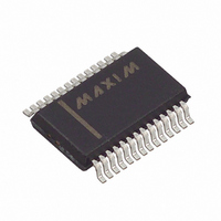
MAX196BCAI+ Maxim Integrated Products, MAX196BCAI+ Datasheet - Page 5

MAX196BCAI+
Manufacturer Part Number
MAX196BCAI+
Description
IC DAS 6CH 12BIT 5V 28-SSOP
Manufacturer
Maxim Integrated Products
Type
Data Acquisition System (DAS)r
Datasheet
1.MAX196BCAI.pdf
(16 pages)
Specifications of MAX196BCAI+
Resolution (bits)
12 b
Sampling Rate (per Second)
100k
Data Interface
Parallel
Voltage Supply Source
Single Supply
Voltage - Supply
4.75 V ~ 5.25 V
Operating Temperature
0°C ~ 70°C
Mounting Type
Surface Mount
Package / Case
28-SSOP
Number Of Adc Inputs
1
Architecture
SAR
Conversion Rate
100 KSPs
Resolution
12 bit
Interface Type
Serial
Mounting Style
SMD/SMT
Lead Free Status / RoHS Status
Lead free / RoHS Compliant
ELECTRICAL CHARACTERISTICS (continued)
(V
with 50% duty cycle; T
TIMING CHARACTERISTICS
(V
with 50% duty cycle; T
Note 1:
Note 2:
Note 3:
Note 4:
Note 5:
Note 6:
Note 7:
Note 8:
Note 9:
Note 10: Not subject to production testing. Provided for design guidance only.
Note 11: All input control signals specified with t
Note 12: t
Note 13: t
CS Pulse Width
WR Pulse Width
CS to WR Setup Time
CS to WR Hold Time
CS to RD Setup Time
CS to RD Hold Time
CLK to WR Setup Time
CLK to WR Hold Time
Data Valid to WR Setup
Data Valid to WR Hold
RD Low to Output Data Valid
RD High to Output Disable
RD Low to INT High Delay
DIGITAL OUTPUTS (D11–D0, INT)
Output Low Voltage
Output High Voltage
Three-State Output Capacitance
DD
DD
= 5V ±5%; unipolar/bipolar range; external reference mode, V
= 5V ±5%; unipolar/bipolar range; external reference mode, V
Accuracy specifications tested at V
Rejection test. Tested for the ±10V (MAX196) and ±4.096V (MAX198) input ranges.
External reference: V
Ground “on” channel; sine wave applied to all “off” channels.
Maximum full-power input frequency for 1LSB error with 10ns jitter = 3kHz.
Guaranteed by design. Not tested.
Use static loads only.
Tested using internal reference.
PSRR measured at full-scale.
External acquisition timing: starts at data valid at ACQMOD = low control byte; ends at rising edge of WR with ACQMOD
= high control byte.
PARAMETER
PARAMETER
DO
TR
is defined as the time required for the data lines to change by 0.5V.
is measured with the load circuits of Figure 2 and defined as the time required for an output to cross 0.8V or 2.4V.
_______________________________________________________________________________________
A
A
= T
= T
MIN
MIN
to T
REF
to T
MAX
SYMBOL
MAX
= 4.096V, offset error nulled, ideal last code transition = FS - 3/2LSB.
SYMBOL
t
t
t
t
t
Multirange, Single +5V, 12-Bit DAS
CSWS
CSWH
t
C
CSRS
CSRH
t
CWH
V
t
CWS
t
t
INT1
V
t
t
t
WR
CS
DS
DH
DO
; unless otherwise noted. Typical values are at T
TR
OUT
; unless otherwise noted.)
OH
OL
DD
Figure 2, C
(Note 13)
V
V
(Note 5)
= 5.0V. Performance at power-supply tolerance limits guaranteed by Power-Supply
R
DD
DD
= t
= 4.75V, I
= 4.75V, I
F
= 5ns from a voltage level of 0.8V to 2.4V.
L
= 100pF (Note 12)
SINK
SOURCE
CONDITIONS
with 12-Bit Bus Interface
CONDITIONS
= 1.6mA
REF
REF
= 1mA
= 4.096V; 4.7µF at REF pin; external clock, f
= 4.096V; 4.7µF at REF pin; external clock, f
A
= +25°C.)
V
MIN
DD
MIN
80
80
60
0
0
0
0
0
- 1
TYP
TYP
MAX
100
120
120
MAX
50
70
0.4
15
CLK
CLK
= 2.0MHz
= 2.0MHz
UNITS
UNITS
ns
ns
ns
ns
ns
ns
ns
ns
ns
ns
ns
ns
ns
pF
V
V
5


