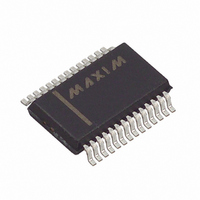
MAX196BCAI+ Maxim Integrated Products, MAX196BCAI+ Datasheet - Page 13

MAX196BCAI+
Manufacturer Part Number
MAX196BCAI+
Description
IC DAS 6CH 12BIT 5V 28-SSOP
Manufacturer
Maxim Integrated Products
Type
Data Acquisition System (DAS)r
Datasheet
1.MAX196BCAI.pdf
(16 pages)
Specifications of MAX196BCAI+
Resolution (bits)
12 b
Sampling Rate (per Second)
100k
Data Interface
Parallel
Voltage Supply Source
Single Supply
Voltage - Supply
4.75 V ~ 5.25 V
Operating Temperature
0°C ~ 70°C
Mounting Type
Surface Mount
Package / Case
28-SSOP
Number Of Adc Inputs
1
Architecture
SAR
Conversion Rate
100 KSPs
Resolution
12 bit
Interface Type
Serial
Mounting Style
SMD/SMT
Lead Free Status / RoHS Status
Lead free / RoHS Compliant
At power-up, the internal power-on reset circuitry sets
INT high and puts the device in normal operation/exter-
nal clock mode. This state is selected to keep the inter-
nal clock from loading the external clock driver when
the part is used in external clock mode.
The MAX196/MAX198 can operate with either an inter-
nal or external reference. An external reference can be
connected to either the REF pin or the REFADJ pin
(Figure 9).
To use the REF input directly, disable the internal buffer
by tying REFADJ to V
nates the need to buffer the reference externally. When
the reference is applied at REFADJ, bypass REFADJ with
a 0.01µF capacitor to AGND.
The REFADJ internal buffer gain is trimmed to 1.6384 to
provide 4.096V at the REF pin from a 2.5V reference.
The internally trimmed 2.50V reference is gained
through the REFADJ buffer to provide 4.096V at REF.
Bypass the REF pin with a 4.7µF capacitor to AGND
and the REFADJ pin with a 0.01µF capacitor to AGND.
The internal reference voltage is adjustable to ±1.5%
(±65 LSBs) with the reference-adjust circuit of Figure 1.
At REF and REFADJ, the input impedance is a mini-
mum of 10kΩ for DC currents. During conversions, an
external reference at REF must be able to deliver
400µA DC load currents, and must have an output
impedance of 10Ω or less. If the reference has higher
output impedance or is noisy, bypass it close to the
REF pin with a 4.7µF capacitor to AGND.
With an external reference voltage of less than 4.096V
at the REF pin or less than 2.5V at the REFADJ pin, the
increase in the ratio of the RMS noise to the LSB value
(FS / 4096) results in performance degradation (loss of
effective bits).
To save power, you can put the converter into low-
current shutdown mode between conversions. Two
programmable power-down modes are available:
STBYPD and FULLPD. Select STBYPD or FULLPD by
programming PD0 and PD1 in the input control byte.
When power-down is asserted, it becomes effective
only after the end of conversion. In all power-down
modes, the interface remains active and conversion
__________Applications Information
Internal or External Reference
______________________________________________________________________________________
DD
. Using the REFADJ input elimi-
Power-Down Mode
Multirange, Single +5V, 12-Bit DAS
Power-On Reset
External Reference
Internal Reference
with 12-Bit Bus Interface
Figure 9a. Internal Reference
Figure 9b. External Reference, Reference at REF
Figure 9c. The external reference overdrives the internal refer-
ence.
MAX196
MAX198
MAX196
MAX198
MAX196
MAX198
2.5V
2.5V
2.5V
10k
10k
10k
A
A
A
V
V
V
= 1.638
= 1.638
= 1.638
REFADJ
REFADJ
REFADJ
REF
REF
REF
26
25
26
25
26
25
4.096V
4.096V
4.7 F
C
REF
V
4.7 F
C
0.01 F
4.7 F
C
0.01 F
DD
REF
REF
4.096V
2.5V
13


