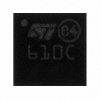
STMPE610QTR STMicroelectronics, STMPE610QTR Datasheet - Page 12

STMPE610QTR
Manufacturer Part Number
STMPE610QTR
Description
IC CTLR ADV TOUCH SCREEN 16-QFN
Manufacturer
STMicroelectronics
Series
S-Touch™r
Type
Resistiver
Specifications of STMPE610QTR
Touch Panel Interface
4-Wire
Number Of Inputs/keys
1 TSC
Resolution (bits)
12 b
Data Interface
I²C, Serial, SPI™
Data Rate/sampling Rate (sps, Bps)
180k
Voltage Reference
External
Voltage - Supply
1.65 V ~ 3.6 V
Operating Temperature
-40°C ~ 85°C
Mounting Type
Surface Mount
Package / Case
16-QFN
Voltage Supply Source
Single Supply
Sampling Rate (per Second)
180k
Resolution
12 bit
Number Of Adc Inputs
6
Interface Type
I2C, SPI
Supply Voltage (max)
3.6 V
Supply Voltage (min)
1.65 V
Maximum Operating Temperature
+ 85 C
Minimum Operating Temperature
- 40 C
Mounting Style
SMD/SMT
Lead Free Status / RoHS Status
Lead free / RoHS Compliant
Other names
497-8825-2
Available stocks
Company
Part Number
Manufacturer
Quantity
Price
SPI interface
5
5.1
5.1.1
12/56
SPI interface
The SPI interface in STMPE610 uses a 4-wire communication connection (DATA IN, DATA
OUT, CLK, CS). In the diagram, “Data in” is referred to as MOSI (master out slave in) and
“DATA out” is referred to as MISO (master in slave out).
SPI protocol definition
The SPI (serial peripheral interface) follows a byte sized transfer protocol. All transfers begin
with an assertion of CS_n signal (falling edge). The protocol for reading and writing is
different and the selection between a read and a write cycle is dependent on the first
captured bit on the slave device. A '1' denotes a read operation and a '0' denotes a write
operation. The SPI protocol defined in this section is shown in Figure 3.
The following are the main features supported by this SPI implementation.
●
●
●
●
●
●
Register read
The following steps need to be followed for register read through SPI.
1.
2.
3.
4.
5.
6.
7.
Support of 1 MHz maximum clock frequency.
Support for autoincrement of address for both read and write.
Full duplex support for read operation.
Daisy chain configuration support for write operation.
Robust implementation that can filter glitches of up to 50 ns on the CS_n and SCL pins.
Support for all 4 modes of SPI as defined by the CPHA, CPOL bits on SPICON.
Assert CS_n by driving a '0' on this pin.
Drive a '1' on the first SCL launch clock on MOSI to select a read operation.
The next 7 bits on MOSI denote the 7-bit register address (MSB first).
The next address byte can now be transmitted on the MOSI. If the autoincrement bit is
set, the following address transmitted on the MOSI is ignored. Internally, the address is
incremented. If the autoincrement bit is not set, then the following byte denotes the
address of the register to be read next.
Read data is transmitted by the slave device on the MISO (MSB first), starting from the
launch clock following the last address bit on the MOSI.
Full duplex read operation is achieved by transmitting the next address on MOSI while
the data from the previous address is available on MISO.
To end the read operation, a dummy address of all 0's is sent on MOSI.
Doc ID 15432 Rev 3
STMPE610


