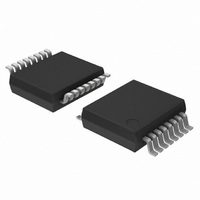
UDA1361TS/N1,112 NXP Semiconductors, UDA1361TS/N1,112 Datasheet - Page 5

UDA1361TS/N1,112
Manufacturer Part Number
UDA1361TS/N1,112
Description
IC ADC STEREO AUDIO 24BIT 16SSOP
Manufacturer
NXP Semiconductors
Type
Stereo Audior
Datasheet
1.UDA1361TSN1118.pdf
(18 pages)
Specifications of UDA1361TS/N1,112
Package / Case
16-SSOP
Resolution (bits)
24 b
Sampling Rate (per Second)
110k
Data Interface
Serial
Voltage Supply Source
Analog and Digital
Voltage - Supply
2.4 V ~ 3.6 V
Operating Temperature
-40°C ~ 85°C
Mounting Type
Surface Mount
Resolution
24 bit
Operating Supply Voltage
2.4 V to 3.6 V
Mounting Style
SMD/SMT
Operating Temperature Range
- 40 C to + 85 C
Supply Current
10.5 mA
Lead Free Status / RoHS Status
Lead free / RoHS Compliant
Lead Free Status / RoHS Status
Lead free / RoHS Compliant, Lead free / RoHS Compliant
Other names
568-1158-5
935267099112
UDA1361TSDK
935267099112
UDA1361TSDK
Available stocks
Company
Part Number
Manufacturer
Quantity
Price
Company:
Part Number:
UDA1361TS/N1,112
Manufacturer:
MICROCHIP
Quantity:
85
NXP Semiconductors
FUNCTIONAL DESCRIPTION
System clock
The UDA1361TS accommodates master and slave
modes. The system devices must provide the system clock
regardless of master or slave mode. In the master mode a
system clock frequency of 256f
mode a system frequency of 256, 384, 512 or 768f
automatically detected (for a system clock of 768f
sampling frequency must be limited to 55 kHz). The
system clock must be locked in frequency to the digital
interface input signals.
Input level
The overall system gain is proportional to V
accurately the potential difference between the reference
voltages V
THD + N/S is specified corresponds to −1 dB(FS) digital
output (relative to the full-scale swing). With an input gain
switch, the input level can be calculated as follows:
at 0 dB gain:
at 6 dB gain:
In applications where a 2 V (RMS) input signal is used, a
12 kΩ resistor must be connected in series with the input
of the ADC. This forms a voltage divider together with the
internal ADC resistor and ensures that only 1 V (RMS)
maximum is input to the IC.
Using this application for a 2 V (RMS) input signal, the gain
switch must be set to 0 dB. When a 1 V (RMS) input signal
is input to the ADC in the same application the gain switch
must be set to 6 dB.
An overview of the maximum input voltage allowed against
the presence of an external resistor and the setting of the
gain switch is given in Table 1. The power supply voltage
is assumed to be 3 V.
2002 Nov 25
96 kHz sampling 24-bit stereo audio ADC
VRP
V
V
and V
i
i
– (
– (
1 dB
1 dB
VRN
)
)
. The −1 dB input level at which
=
=
V
--------------------------------- -
V
--------------------------------- -
VRP
VRP
s
2
is required. In the slave
–
3
–
×
V
V
3
VRN
VRN
=
=
DDA
V (RMS)
V (RMS)
, or more
s
s
the
is
5
Table 1 Application modes using input gain stage
Multiple format output interface
The serial interface provides the following data output
formats in both master and slave modes
(see Figs 3, 4 and 5):
• I
• MSB-justified serial format with data word length of up to
The master mode drives pins WS (word select; 1f
BCK (bit clock; 64f
mode.
Table 2 Master/slave select
Table 3 Select data format
Decimation filter
The decimation from 64f
first stage realizes a 4th-order sinx/x characteristic. This
filter decreases the sample rate by 8.
The second stage, a FIR filter, consists of 3 half-band
filters, each decimating by a factor of 2.
Present
Present
Absent
Absent
24 bits.
2
RESISTOR
S-bus with data word length of up to 24 bits
(12 kΩ)
MSSEL
SFOR
M
M
H
H
L
L
s
). WS and BCK are received in slave
INPUT GAIN
s
SWITCH
is performed in two stages. The
0 dB
0 dB
0 dB
6 dB
slave mode
master mode
(reserved for digital test)
I
MSB-justified data format
(reserved for analog test)
2
S-bus data format
MASTER/SLAVE
DATA FORMAT
UDA1361TS
Product specification
SELECT
MAXIMUM
VOLTAGE
INPUT
(RMS)
0.5 V
2 V
1 V
1 V
s
) and


