ADC12441CIJ National Semiconductor, ADC12441CIJ Datasheet - Page 3
ADC12441CIJ
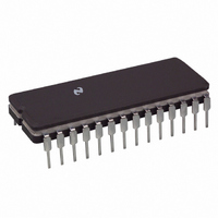
Manufacturer Part Number
ADC12441CIJ
Description
IC ADC 12BIT DYNAM TEST 28CDIP
Manufacturer
National Semiconductor
Datasheet
1.ADC12441CIJ.pdf
(14 pages)
Specifications of ADC12441CIJ
Number Of Bits
12
Sampling Rate (per Second)
55k
Data Interface
Parallel
Number Of Converters
2
Power Dissipation (max)
70mW
Voltage Supply Source
Analog and Digital, Dual ±
Operating Temperature
-40°C ~ 85°C
Mounting Type
Through Hole
Package / Case
28-CDIP (0.600", 15.24mm)
Lead Free Status / RoHS Status
Contains lead / RoHS non-compliant
Other names
*ADC12441CIJ
Available stocks
Company
Part Number
Manufacturer
Quantity
Price

Part Number:
ADC12441CIJ
Manufacturer:
NS/国半
Quantity:
20 000


DYNAMIC CHARACTERISTICS (Continued)
Symbol
THD
THD
Symbol
V
V
I
I
V
V
V
V
V
Converter Electrical Characteristics
The following specifications apply for V
Impedance
all other limits T
Digital and DC Electrical Characteristics
The following specifications apply for DV
otherwise specified Boldface limits apply for T
(Notes 6 and 7)
IN(1)
IN(0)
IN(1)
IN(0)
T
T
H
OUT(1)
OUT(0)
b
a
Bipolar Total Harmonic Distortion
(Note 17)
Unipolar Total Harmonic Distortion
(Note 17)
Bipolar Peak Harmonic or
Spurious Noise (Note 17)
Unipolar Peak Harmonic or
Spurious Noise (Note 17)
Bipolar Two Tone Intermodulation
Distortion (Note 17)
Unipolar Two Tone Intermodulation
Distortion (Note 17)
Aperture Time
Aperture Jitter
b
b
3 dB Bipolar Full Power Bandwidth
3 dB Unipolar Full Power Bandwidth
e
Logical ‘‘1’’ Input Voltage for
All Inputs except CLK IN
Logical ‘‘0’’ Input Voltage for
All Inputs except CLK IN
Logical ‘‘1’’ Input Current
Logical ‘‘0’’ Input Current
CLK IN Positive-Going
Threshold Voltage
CLK IN Negative-Going
Threshold Voltage
CLK IN Hysteresis
Logical ‘‘1’’ Output Voltage
Logical ‘‘0’’ Output Voltage
V
600
T
A
a
e
(min)
T
and f
Parameter
J
e
b
Parameter
CLK
25 C (Notes 6 7 and 8) (Continued)
V
T
b
e
(max)
2 0 MHz unless otherwise specified Boldface limits apply for T
CC
CC
e
e
DV
V
V
V
V
V
V
AV
CC
CC
CC
IN
IN
CC
CC
A
I
I
OUT
OUT
CC
e
e
e
e
e
e
e
e
e a
T
5V
0V
5 25V
4 75V
4 75V
e b
e b
4 75V I
AV
J
f
f
f
f
f
f
f
f
f
f
V
f
V
f
V
V
Conditions
IN
IN
IN
IN
IN
IN
IN
IN
IN
IN
IN2
IN2
IN
IN
IN
IN
e
CC
5 0V V
e
e
e
e
e
e
e
e
e
e
360 A
10 A
e
e
e
e
e
e
T
e a
MIN
1 kHz V
19 688 kHz V
1 kHz V
19 688 kHz V
1 kHz V
10 kHz V
20 kHz V
1 kHz V
10 kHz V
20 kHz V
OUT
3
4 85 V
4 85 V
g
g
20 625 kHz
20 625 kHz
4 85V f
4 85V (Note 17)
to T
b
5 0V V
e
Conditions
p-p
p-p
e b
1 6 mA
IN
IN
IN
IN
MAX
IN
IN
IN
IN
(Note 17)
IN1
e
e
e
e
f
IN1
e
e
e
e
b
5 0V V
4 85 V
4 85 V
g
IN
IN
g
all other limits T
e
4 85 V
4 85 V
e b
g
g
e
4 85V
4 85V
e
e
4 85V
4 85V
19 375 kHz
19 375 kHz
4 85 V
g
REF
p-p
p-p
5 0V V
(Note 9)
Typical
b
p-p
p-p
4 85V
0 005
0 005
2 8
2 1
0 7
e a
p-p
REF
5 0V and f
A
(Note 9) (Notes 10 19)
Typical
e a
e
b
b
b
b
b
b
b
b
b
b
b
b
100
100
25
30
(Notes 10 19)
T
82
80
82
80
88
84
80
90
86
82
78
78
J
5 0V Analog Input Source
A
e
Limit
e
2 0
0 8
2 7
2 3
0 4
2 4
4 5
0 4
b
CLK
1
25 C
1
T
J
e
Limit
b
b
b
b
e
20
20
75
75
74
73
2 0 MHz unless
T
MIN
to T
(Limits)
V (max)
V (max)
V (max)
V (min)
V (min)
V (min)
V (min)
V (min)
A (max)
A (max)
Units
kHz (Min)
kHz (Min)
dB (max)
dB (max)
dB (max)
dB (max)
(Limit)
Units
ps
MAX
dB
dB
dB
dB
dB
dB
dB
dB
ns
rms
Related parts for ADC12441CIJ
Image
Part Number
Description
Manufacturer
Datasheet
Request
R

Part Number:
Description:
National Semiconductor [8-Bit D/A Converter]
Manufacturer:
National Semiconductor
Datasheet:
Part Number:
Description:
National Semiconductor [Media Coprocessor]
Manufacturer:
National Semiconductor
Datasheet:
Part Number:
Description:
Digitally Controlled Tone and Volume Circuit with Stereo Audio Power Amplifier, Microphone Preamp Stage and National 3D Sound
Manufacturer:
National Semiconductor
Datasheet:
Part Number:
Description:
Digitally Controlled Tone and Volume Circuit with Stereo Audio Power Amplifier, Microphone Preamp Stage and National 3D Sound
Manufacturer:
National Semiconductor
Datasheet:
Part Number:
Description:
AC97 Rev 2 Codec with Sample Rate Conversion and National 3D Sound
Manufacturer:
National Semiconductor
Part Number:
Description:
Manufacturer:
National Semiconductor
Datasheet:
Part Number:
Description:
Manufacturer:
National Semiconductor
Datasheet:
Part Number:
Description:
General Purpose, Low Voltage, Low Power, Rail-to-Rail Output Operational Amplifiers
Manufacturer:
National Semiconductor
Datasheet:
Part Number:
Description:
8-bit 20 MSPS flash A/D converter.
Manufacturer:
National Semiconductor
Datasheet:
Part Number:
Description:
Low Noise Quad Operational Amplifier
Manufacturer:
National Semiconductor
Datasheet:
Part Number:
Description:
Quad Differential Line Receivers
Manufacturer:
National Semiconductor
Datasheet:
Part Number:
Description:
Quad High Speed Trapezoidal? Bus Transceiver
Manufacturer:
National Semiconductor
Datasheet:
Part Number:
Description:
Dual Line Receiver
Manufacturer:
National Semiconductor
Datasheet:
Part Number:
Description:
TTL to 10k ECL Level Translator with Latch
Manufacturer:
National Semiconductor
Datasheet: